


1. Introduction
Plasmons are charge oscillations in the interface of metals and dielectrics. They were discussed firstly in the visible region of the spectrum of electromagnetic fields. Thereafter, they were studied in other parts of the spectrum such as infrared (IR) and terahertz bands. When the plasmons accumulate around metallic nanoparticles, the local field increases and also, they have the ability to propagate along the metal-dielectric boundary. This is known as surface plasmon polariton (SPP). The characteristics of surface plasmons has led to the formation of the Plasmonics. Among the first studies in this topic we may point to light propagations through the subwavelength aperture reported in 1988 [1], thereafter the topic grew rapidly.
SPPs have the most interesting applications in integrated optical circuits and devices [2, 3], such as subwavelength waveguides [4, 5], switches [6–9], sensors [10–13], biosensors [14], graphene plasmonic meta-surfaces [15], U-shaped waveguides [16], waveguide couplers [17–19], metal-dielectric-metal waveguides [20–23], plasmonic metal–insulator-semiconductor waveguides [24], metal–insulator-semiconductor-metal waveguides [25] detectors [26, 27], plasmonic amplifiers [28, 29], signal amplifiers [30], solar cells [31], resonators [32–34] and demultiplexers [35–37].
Two types of filters are discussed by researchers: band pass filters BPF and band stop filters. BPFs are usually realized using a cavity which is coupled to two waveguides. When the resonance frequency of the cavity matches the frequency of the guiding mode, the mode can propagate through the filter, otherwise light cannot pass through the filter. The study on plasmonic filters has been expanded in recent years [38–41]. One of the benefits of plasmonic devices is requiring less area than similar photonic crystal devices [42–56]. It is necessary to use finite-difference-time-domain (FDTD) method, in order to investigate plasmonic filters.
We can design single mode [57] or multi-mode filters [58] using plasmonic structures. In this paper, four dual-mode filters with different resonator shapes (circle, square, rhombus, and hexagon) have been presented. In order to improve the filter's performance, two triangular-shaped adjunctions have been added to the input and output waveguides. As will be seen, each of proposed structures has a better transmission than the previous structures. That means a higher peak of transmittance is obtained. By changing the parameters of the structures in these filters, different resonant wavelengths can be obtained. Our new designs demonstrate the better frequency response while having smaller dimensions. The proposed structures have been simulated by using FDTD method.
2. Basic filter topologies
In this section, we first concentrate on a simple narrow band pass filter in which there is a metal–insulator–metal (MIM) waveguide consisting of a nanodisk resonator in the middle of the structure. The characteristics of the filter can be tuned by changing the dimensions. The wavelengths of the resonant modes are calculated by resonant theory and verified by FDTD method [59]. The structure will be theoretically investigated in sections 3 and 4 . The result of FDTD exactly matches with the theory results. The structure of initial plasmonic band pass filter is shown in figure 1(a). It consists of two slits (two semi-infinite waveguides at the right and left) and a nanodisk resonator as a cavity between them. We have also introduced other filters with different resonator shapes such as figures 1(b)–(d).
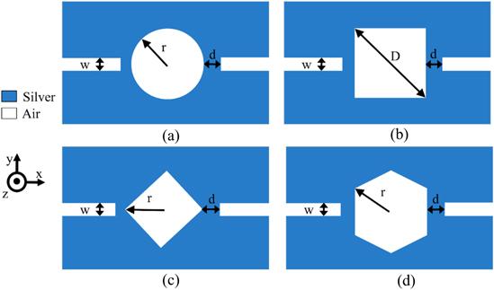
Figure 1. Schematic diagram of plasmonic BPF: (a) with a circular resonator (filter 1), (b) with a square-shaped resonator (filter 2), (c) with a resonator in a form of rhombus (filter 3), (d) with a hexagonal resonator (filter 4). |
The cavity and slits are set as air with relative permittivity of (${\varepsilon }_{d}=1$), the radius of circular nanodisk is r = 200 nm, the width of waveguide is w = 50 nm, the coupling distance between cavity and waveguides is d = 20 nm. The three other filters (figures 1(b)–(d)) have the same characteristics with the first filter in figure 1(a). The only difference between them is the radius or diagonal of these resonators. In these four structures, the area of resonators is approximately equal to each other. These structures are supposed to be uniform along z direction (z-axis), so we can simplify them into 2D-FDTD that means $\tfrac{\partial }{\partial z}=0$ [60, 61].
Figure 2 shows the Lorentzian transmission spectrum of these filters. There are two assumptions in these filters: these structures can be designed by considering the same area of resonators or the same distance between the waveguides. In the primary design of filters, the radius of circle, the diagonal of square, the radius of rhombus, and the radius of hexagon have been set to 200 nm, 255 nm, 200 nm, and 230 nm, respectively which the vertical edges of hexagon and square have been placed in the same coordinate of two vertices in rhombus as their transmittance spectra have been exhibited in figure 2. The first and second modes of the filter 1 are at the wavelengths of 806 and 518 nm, filter 2 is at the wavelength of 865 nm, filter 3 and filter 4 are at the wavelength of 713 and 555 nm, and 844 and 550 nm, respectively.
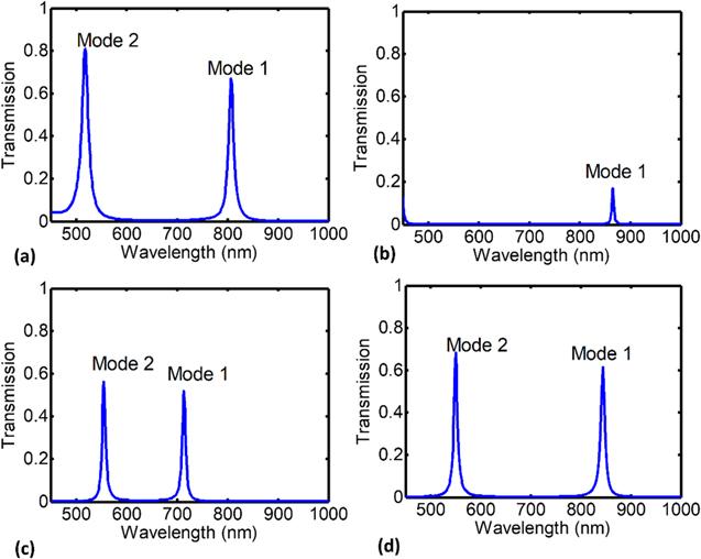
Figure 2. Transmission spectrum of the structures of figure 1 with the primary design which is comprised of two resonance mode using the Drude model: (a) resonator of filter 1 with the radius of r = 200 nm- peak transmission (0.67, 0.81), (b) resonator of filter 2 with the diagonal of D = 510 nm or x-coordinate of vertical edge in 180 nm peak transmission (0.17), (c) resonator of filter 3 with the radius of r = 200 nm- peak (0.52, 0.56), (d) resonator of filter 4 with the radius of r = 230 nm or x-coordinate of vertical edge in 200 nm- peak (0.61, 0.68). |
Optimized geometry of the structures in figure 1 have been proposed as called secondary design and the results have been shown in figure 3. In the secondary design, the vertical edge of square or hexagon in the filter 2 or filter 3 is in such a way that its distance from the waveguides is equal to the separation in the first simple filter. In the same way, the hexagonal resonator in the fourth filter also has the same radius of the circle in the first resonator. The frequency responses have been presented in figure 3. Each of these four filters have two modes (mode 1 and mode 2). The first and second modes of the filter 1, 2, 3, and 4 are at the wavelengths of 857 and 541 nm, 999 and 496 nm, 759 and 586 nm, and 885 and 572 nm, respectively.
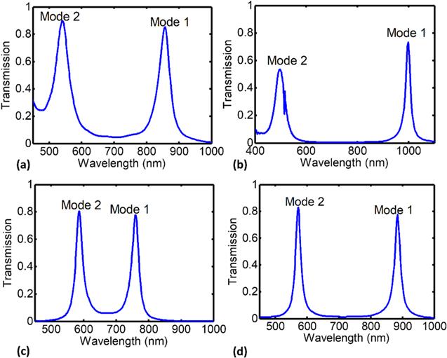
Figure 3. Transmission spectrum of the structures of figure 1 which is comprised of two resonance mode of the maximum possible transmission in the structure in terms of dimension (secondary design): (a) resonator of filter 1 with the radius of r = 210 nm- peak (0.85, 0.897), (b) resonator of filter 2 with the diagonal of D = 594 nm or x-coordinate of vertical edge in 210 nm- peak (0.73, 0.53), (c) resonator of filter 3 with the radius of r = 210 nm- peak (0.78, 0.80), (d) resonator of filter 4 with the radius of r = 240 nm or x-coordinate of vertical edge in 210 nm- peak (0.77, 0.83). |
3. Modeling of the filtering structures
There are several models that describe the optical response of silver in the structures of figure 1. The models can be expressed as follows:
3.1. Drude model
The permittivity of silver is approximated via a Drude model as below [62]:
$ \begin{eqnarray}\varepsilon \left(\omega \right)={\varepsilon }_{\infty }-\displaystyle \frac{{\omega }_{p}^{2}}{{\omega }^{2}+{\rm{i}}\gamma \omega },\end{eqnarray}$
where ${\varepsilon }_{\infty }$ is the dielectric constant at the infinite frequency and can be assumed as (${\varepsilon }_{\infty }=3.7$) in the Drude model, ${\omega }_{p}$ is the plasma frequency (${\omega }_{p}=9.1$ eV), γ is the electron collision frequency (γ = 0.081 eV), and ω is the angular frequency of incident light.3.2. Drude–Lorentz model
In this section, the transmission of this waveguide can be determined by a seven-pole Drude–Lorentz model which is accurate in the wavelength range from 200 to 2000 nm [63]
$ \begin{eqnarray}{\varepsilon }_{m}\left(\omega \right)=1-\displaystyle \frac{{\omega }_{p}^{2}}{\omega \left(\omega +j\gamma \right)}+\displaystyle \sum _{n=1}^{5}\displaystyle \frac{{f}_{n}\,{\omega }_{n}^{2}}{{\omega }_{n}^{2}-{\omega }^{2}-j\omega {\gamma }_{n}\,},\end{eqnarray}$
where ${\omega }_{p}=2002.6$ THz is the plasma frequency of silver and $\gamma =11.61$ THz is a damping constant. Table 1 summarizes the other parameters.Table 1. Parameters of Drude–Lorentz model for silver. |
| n | ${\omega }_{n}({\rm{THz}})$ | ${\gamma }_{n}({\rm{THz}})$ | ${f}_{n}$ |
|---|---|---|---|
| 1 | 197.3 | 939.62 | 7.9247 |
| 2 | 1083.5 | 109.29 | 0.5013 |
| 3 | 1979.1 | 15.71 | 0.0133 |
| 4 | 4392.5 | 221.49 | 0.8266 |
| 5 | 9812.1 | 584.91 | 1.1133 |
3.3. Palik model
The last model is named the Palik model which specifies the permittivity of silver in a wider range of wavelength.
4. Theoretical investigation
This section consists of a study on the main theory in basic filter topologies and a discussion of theory about the tapered shaped structures.
4.1. Main discussion on the theory
Firstly, the circular resonator has been investigated. The nanocavity resonance condition for disk-shaped resonator can be given through the bellow equations which include the incident, scattered and transmitted fields by use of subscripts i, s, and t, respectively [64]3 ) and (4 ) as shown below:
$ \begin{eqnarray}{a}_{n}^{i}{K}_{d}{J}_{n}\left({K}_{d}r\right)+{a}_{n}^{s}{K}_{d}{H}_{n}^{\left(1\right)}\left({K}_{d}r\right)={a}_{n}^{t}{K}_{m}{J}_{n}\left({K}_{m}r\right),\end{eqnarray}$
$ \begin{eqnarray}\begin{array}{l}{\eta }_{d}{K}_{d}{a}_{n}^{i}\,{J}_{n}^{{\prime} }\left({K}_{d}r\right)+{\eta }_{d}{K}_{d}{a}_{n}^{s}{H}_{n}^{{\prime} \left(1\right)}\left({K}_{d}r\right)\\ \,=\,{\eta }_{d}{K}_{m}{a}_{n}^{t}{J}_{n}^{{\prime} }\left({K}_{m}r\right),\end{array}\end{eqnarray}$
where ${K}_{m}=K{\left({\varepsilon }_{m}\right)}^{\tfrac{1}{2}}$ and ${K}_{d}=K{\left({\varepsilon }_{d}\right)}^{\tfrac{1}{2}}$ are the wave vectors in metal and dielectric, $K$ is the wave vector, ${\varepsilon }_{m}$ and ${\varepsilon }_{d}$ denote the relative permittivity of metal and dielectric respectively, and r is the radius of nanocavity. ${J}_{n}$ and ${J}_{n}^{\prime} $ are the first kind Bessel function and its derivation and the index of n represents the order of this function. ${H}_{n}^{(1)}$ and ${H}_{n}^{{\prime} (1)}$ are the first kind Hankel functions with the order n and its derivation. ${a}_{n}^{i},$ ${a}_{n}^{s},$ and ${a}_{n}^{t}$ show the amplitudes of the incident, scattered and transmitted field, respectively. The resonance condition can be obtained by applying the boundary conditions for magnetic and electric fields and by solving the equations ( $ \begin{eqnarray}{K}_{d}\displaystyle \frac{{H}_{n}^{{\prime} \left(1\right)}\left({K}_{m}r\right)}{{H}_{n}^{\left(1\right)}\left({K}_{m}r\right)}={K}_{m}\displaystyle \frac{{J}_{n}^{{\prime} }\left({K}_{d}r\right)}{{J}_{n}\left({K}_{d}r\right)}.\end{eqnarray}$
Assuming δ to be the normalized frequency $\omega ,$ which is defined by $\delta =\tfrac{\omega -{\omega }_{0}}{{\omega }_{0}},$ whereas ω represents the frequency of the incident light, and ${\omega }_{0}$ presents the resonant frequency. The transfer function (t) at the transmitted port of the filter can be determined according to the following equation:
$ \begin{eqnarray}t=\displaystyle \frac{\tfrac{1}{{Q}_{w}}}{j2\delta +\tfrac{1}{{Q}_{i}}+\tfrac{1}{{Q}_{w}}},\end{eqnarray}$
where ${Q}_{i}=\tfrac{{\omega }_{0}{\tau }_{i}}{2}$ and ${Q}_{w}=\tfrac{{\omega }_{0}{\tau }_{w}}{2}$ are quality factors of cavity which are related to intrinsic loss and waveguide coupling loss. $\tfrac{1}{{\tau }_{{\rm{i}}}}$ stands for the decay rate of the electromagnetic filed due to internal loss in the nanodisk resonator and $\tfrac{1}{{\tau }_{\omega }}$ is the decay rate of power escape through the waveguides. As a result, the transmission spectrum around the resonant modes shows Lorentzian profiles. The transmission can be calculated as: $ \begin{eqnarray}T=\left|{t}^{2}\right|=\displaystyle \frac{{\left(\tfrac{1}{{\tau }_{\omega }}\right)}^{2}}{{\left(\omega -{\omega }_{0}\right)}^{2}+{\left(\tfrac{1}{{\tau }_{{\rm{i}}}}+\tfrac{1}{{\tau }_{\omega }}\right)}^{2}}.\end{eqnarray}$
4.2. Theoretical investigation of tapered transmission line (TTL)
A main MIM filter structure has been investigated which includes a cavity connected to two waveguides by transmission line model [8]. The structure will be modeled with transmission line (TL) as shown in figure 4. The two waveguides at left and right side of the MIM structure have been assumed to be identical in length and width (${l}_{1}={l}_{2}\,{\rm{and}}\,{w}_{1}=w2$). The width and length of the cavity are ${l}_{c}\,{\rm{and}}\,{w}_{c},$ respectively. The characteristic impedance of ${Z}_{i}$ ($i=1,2$) has been considered as a model of waveguides in TL in order to achieve transmission function by employing transfer matrix. The transfer matrix will be obtained from the corresponding scattering matrix which has a relation between input and output ports. Thus, the transfer matrix will be defined as:
$ \begin{eqnarray}\begin{array}{c}T=\left[\begin{array}{cc}{t}_{11} & {t}_{12}\\ {t}_{12} & {t}_{11}\end{array}\right]=\displaystyle \frac{1}{{S}_{21}}\left[\begin{array}{cc}1 & -{s}_{22}\\ {s}_{11} & -{\rm{Det}}(S)\end{array}\right],\end{array}\end{eqnarray}$
where the elements of the matrix will be described as: $ \begin{eqnarray}{t}_{11}=\displaystyle \frac{1}{2}\left(\sqrt{\displaystyle \frac{{z}_{2}}{{z}_{1}}}+\sqrt{\displaystyle \frac{{z}_{1}}{{z}_{2}}}\right)\,,\,{t}_{12}=\displaystyle \frac{1}{2}\left(\sqrt{\displaystyle \frac{{z}_{2}}{{z}_{1}}}-\sqrt{\displaystyle \frac{{z}_{1}}{{z}_{2}}}\right)\,.\end{eqnarray}$
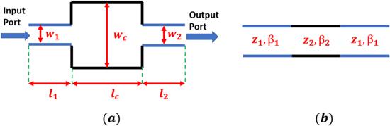
Figure 4. (a) Schematic view of MIM junction, (b) equivalent transmission line model. |
The elements of the scattering matrix will also be as:
$ \begin{eqnarray}{s}_{11}=-{s}_{22}={\rm{\Gamma }},\,{s}_{12}={s}_{21}=\displaystyle \frac{2\sqrt{{z}_{1}{z}_{2}}}{{z}_{1}+z\_2},\end{eqnarray}$
where ${\rm{\Gamma }}=\tfrac{{z}_{2-}{z}_{1}}{{z}_{2}+{z}_{1}},$ and the scattering matrix of a direct junction and a straight waveguide of length L are can be specified as ${S}_{{\rm{j}}{\rm{u}}{\rm{n}}}=\left[\begin{array}{ll}{\rm{\Gamma }} & 1-{\rm{\Gamma }}\\ 1+{\rm{\Gamma }} & -{\rm{\Gamma }}\end{array}\right]$ and ${S}_{{\rm{M}}{\rm{I}}{\rm{M}}}=\left[\begin{array}{ll}0 & {{\rm{e}}}^{-{\rm{i}}\beta L}\\ {{\rm{e}}}^{{\rm{i}}\beta L} & 0\end{array}\right],$ respectively. The relationship between input and output voltages with the subscripts (1) and (2) is expressed by: $ \begin{eqnarray}\left[\begin{array}{l}{V}_{1}^{+}\\ {V}_{1}^{-}\end{array}\right]=T\left[\begin{array}{l}{V}_{2}^{+}\\ {V}_{2}^{-}\end{array}\right].\end{eqnarray}$
Finally, the transfer function of the equivalent TL model can be attained as:
$ \begin{eqnarray}T={T}_{1}\left({l}_{1}\right){T}_{{\rm{j}}{\rm{u}}{\rm{n}}1}{T}_{2}\left({l}_{c}\right){T}_{{\rm{j}}{\rm{u}}{\rm{n}}2}{T}_{1}\left({l}_{1}\right),\end{eqnarray}$
where $ \begin{eqnarray}\begin{array}{l}{T}_{j}\left({L}_{j}\right)=\left[\begin{array}{lc}{{\rm{e}}}^{-{\rm{i}}{\beta }_{j}{L}_{j}} & 0\\ 0 & {{\rm{e}}}^{{\rm{i}}{\beta }_{j}{L}_{j}}\end{array}\right],\,{T}_{\mathrm{ju}{\rm{n}}(j)}=\left[\begin{array}{lc}{t}_{j}^{+} & {t}_{j}^{-}\\ {t}_{j}^{-} & {t}_{j}^{+}\end{array}\right],\\ {t}_{j}^{\pm }=\frac{\sqrt{\displaystyle \frac{{z}_{(j+1)}}{{z}_{(j)}}}\pm \sqrt{\displaystyle \frac{{z}_{(j)}}{{z}_{(j+1)}}}}{2}.\end{array}\end{eqnarray}$
The theory can be extended to more cascaded junctions and transmission can be calculated as $T={\left|\tfrac{{V}_{2}^{+}}{{V}_{1}^{+}}\right|}^{2}.$
The theory of TTL can be discussed in the structures with variation of characteristic impedance from ${Z}_{1}\,$ to ${Z}_{2}$ [69, 70]. The schematic view of a TTL has been demonstrated in figure 5. The impedance Z(z) is a function of $z$ and has a step change of ${\rm{d}}z:$
$ \begin{eqnarray}{\rm{d}}{\rm{\Gamma }}=\displaystyle \frac{1}{2}{{\rm{e}}}^{-2{\rm{i}}\beta z}\displaystyle \frac{{\rm{d}}}{{\rm{d}}z}\left(\mathrm{ln}\,\displaystyle \frac{Z}{{Z}_{1}}\right){\rm{d}}z.\end{eqnarray}$
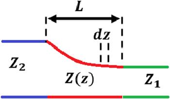
Figure 5. Schematic view of equivalent tapered transmission line (TTL). |
Each reflection coefficient in the small section of length ${\rm{d}}z$ will be achieved as a function of frequency, so the total reflection coefficient will be attained by summing up the partial reflections ${\rm{d}}{\rm{\Gamma }}$ over the length L. Each partial section has its own suitable phase shift that the phase changes continuously during the length. The total reflection coefficient can be defined as follows where ${\theta }_{m}$ represents the total phase shift:
$ \begin{eqnarray}{\rm{\Gamma }}=\displaystyle \frac{1}{2}\displaystyle {\int }_{0}^{{\theta }_{m}}{{\rm{e}}}^{-2{\rm{i}}\theta }\displaystyle \frac{{\rm{d}}}{{\rm{d}}\theta }\left(\mathrm{ln}\,\displaystyle \frac{Z}{{Z}_{1}}\right){\rm{d}}\theta .\end{eqnarray}$
The ${\rm{d}}\left(\mathrm{ln}\,\tfrac{Z}{{Z}_{1}}\right)$ is considered as a triangular function, so we can derive the following equations:
$ \begin{eqnarray}\mathrm{ln}\,\displaystyle \frac{Z}{{Z}_{1}}=\displaystyle \frac{\theta }{{\theta }_{m}}\,\mathrm{ln}\,\displaystyle \frac{{Z}_{2}}{{Z}_{1}},\end{eqnarray}$
$ \begin{eqnarray}Z={Z}_{1}\exp \left(\displaystyle \frac{\theta }{{\theta }_{m}}\,\mathrm{ln}\,\displaystyle \frac{{Z}_{2}}{{Z}_{1}}\right),\end{eqnarray}$
$ \begin{eqnarray}{\rm{\Gamma }}=\displaystyle \frac{1}{2}{{\rm{e}}}^{-{\rm{i}}{\theta }_{m}}\,\mathrm{ln}\left(\displaystyle \frac{{Z}_{2}}{{Z}_{1}}\right)\displaystyle \frac{\sin \,{\theta }_{m}}{{\theta }_{m}}.\end{eqnarray}$
A higher transmission and a wider bandwidth will be obtained with TTL. To achieve higher bandwidth, a multi-section transformer is required therefore the impedance variation of TL will lead to having TTL transformer. By changing the geometry of the structure, the impedance transit will be attained. The results of higher transmission will be shown in section 5 .
5. The proposed structures and their better results
In this section, four optimized optical band pass filters have been proposed. Each of these filters have two propagating SPP modes which have higher transmission peaks corresponding to the resonance wavelength. To achieve a multiband filter with better transmission, two triangular-shaped adjunctions are added to both waveguides at the left and right as was conceptually investigated in section 4 . The schematic of the proposed structures is shown in figure 6. When the optical waves propagate through the waveguide structure, some frequencies of light are permitted to transmit and incident light can pass through the structure. Furthermore, certain frequencies are prohibited from propagating for which the transmission is zero in the spectrum. As seen in section 1 , the filters different topologies have been investigated. In this section, the configurations of filters are investigated with triangular-shaped adjunctions in order to have optimized optical filters. They are shown in figures 6(a)–(d).
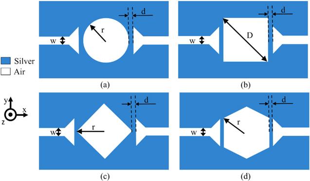
Figure 6. Schematic diagram of the proposed filters with triangular-shaped adjunctions in the: (a) first proposed filter with circular resonator (filter 5), (b) second proposed filter with quadratic resonator (filter 6), (c) Third proposed filter with a resonator in a form of rhombus (filter 7), (d) Fourth proposed filter with hexagonal resonator (filter 8). |
Figures 6(a)–(d) shows four proposed filters. These configurations are used to increase the maximum transmission peaks of the transmittance spectrums. The increment of transmission will be obtained not only by the design of the shape of resonator cavity such as circle, square, rhombus, or hexagon, but by using the two triangular-shaped adjunctions and adjusting the edges of the two triangles in the right and left waveguides. The transmission spectrums of these structures have been calculated and the results have been presented for circular, square and hexagonal resonators with the triangular-shaped adjunctions in figures 7(a)–(d) and 8(a)–(d). The transmission spectrums have been shown in figures 7(a) and 8(a) for the primary and secondary design of the structure, respectively. It can be seen that transmission at the wavelength of mode 2 has a higher peak than the other mode. It is because the decay rate of the field induced by internal loss is larger in mode 2. The filter based on a hexagonal optical resonator has the highest transmission peak. Focusing on the secondary design with better frequency response, the resonance modes of the circular resonator are at the wavelengths of 515 nm and 808 nm and the maximum transmissions of these two modes are 90% and 89% respectively which are higher than the similar filter without triangular-shaped junctions. The resonance modes of quadratic resonator are at the wavelength of 482 nm and 999 nm and the maximum transmissions of these two modes are 67% and 83% and the maximum transmissions of filter 7 are 79% and 78%, respectively. And for the hexagonal resonator, the resonance modes are at the wavelength of 568 nm and 885 nm and the maximum transmissions of these two modes are 86% and 85% respectively. As a result, by focusing among the polygon shapes, the hexagonal resonator with triangular-shaped adjunctions in the waveguides has the higher peak transmission in both of the resonance modes. Figures 8(a)–(d) has been presented for the secondary design of structures.
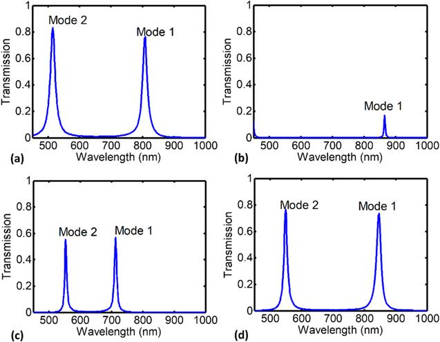
Figure 7. Transmission spectrum of the structures of figure 6 with the primary design of structures mentioned in section |
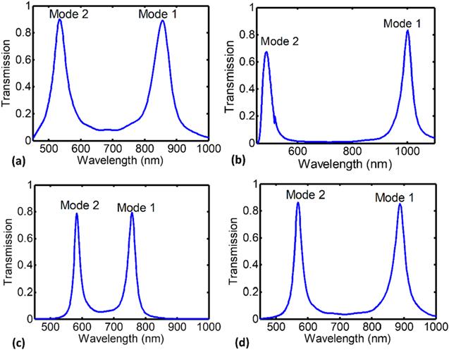
Figure 8. Transmission spectrum of the structures of figure 6 with the secondary design of structures mentioned in section |
For each topology, the magnitude of $\left|{H}_{z}\right|$ has been depicted at the resonance wavelengths (λ1 and λ2) in figure 9. The ‘a' and ‘b' parts correspond to the respective resonance modes. The ‘c' parts correspond to non-resonance wavelengths. As can be seen in the field profile, these two modes can be transmitted to the output in the filter. But the transmission is prohibited at the non-resonance wavelengths like 650 (nm) (see figure 9(c)).
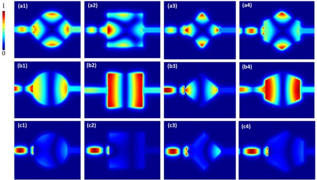
Figure 9. Field distribution of $\left|{{H}}_{{z}}\right|$ for filters with triangular-shaped adjunctions mentioned proposed in figure 6 at the resonance (a), (b) and non-resonance (c) wavelengths of: (1) circular resonator for; (a) λ2 = 515 nm, (b) λ1 = 808 nm, (c) λ = 650 nm. (2) Square-shaped resonator for; (a) λ2 = 482 nm, (b) λ1 = 999 nm, (c) λ = 700 nm. (3) Rhombus-shaped resonator for; (a) λ2 = 582 nm, (b) λ1 = 789 nm, (c) λ = 650 nm. (4) Hexagonal resonator for; (a) λ2 = 568 nm, (b) λ1 = 885 nm, (c) λ = 700 nm. |
Figure 9 exhibits the field distribution of $\left|{H}_{z}\right|$ correspond to the second and first resonances in figure 6. As observed in figure 8(d), the resonance which occurs at the longer wavelength of 885 nm has the lower peak of transmission than the first one. Referring to figure 7, the wavelength of the second mode has more power density than the other one which can be coupled into the middle resonator by more power [71]. The none-resonance wavelength has been chosen at 700 (nm). For this case, the light is prohibited to transmit through the structure.
6. Parametric study on proposed filters
6.1. Effects of the size of resonators
Figure 10 shows the influence of different parameters on the resonance wavelengths and response of these proposed filters. The transmission peaks in the spectrum will be increased by increasing the radius of the resonator in the first filter as seen in figures 10(a) and (b). It is obvious that, the wavelength of the mentioned filter would be gradually increased. The other benefit of this filter is the increment of response by adding the triangular-shaped adjunctions as shown in figure 6(b). In the second optimized filter (filter 6), the transmission peaks will be increased by changing the diagonal of the square or rhombus as shown in figures 10(c)–(f). In this way the resonance mode can be certainly tuned by changing the size of the structures, especially with the parameters of resonator and adjunctions in waveguides. Another proposed filter has a hexagonal resonator as seen in figure 6(d). The response of the filter has been investigated in figures 10(g) and (h).
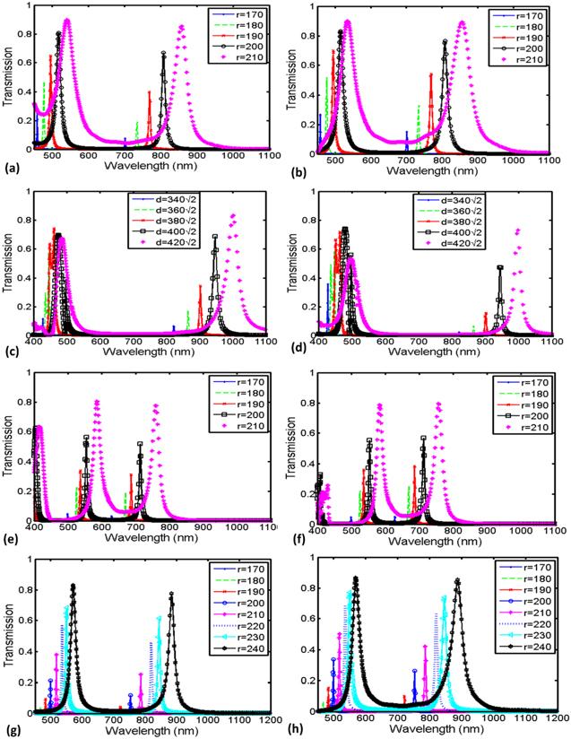
Figure 10. Comparison of transmission of these four proposed filters with or without triangular-shaped adjunctions by applying different parameters in them with: 1-circular resonator (a) without triangular-shaped adjunctions, (b) with triangular-shaped adjunctions; 2-quadratic resonator (c) without triangular-shaped adjunctions, (d) with triangular-shaped adjunctions; 3-rhombus-shaped resonator (e) without triangular-shaped adjunctions, (f) with triangular-shaped adjunctions; 4-hexagonal resonator (e) without triangular-shaped adjunctions, (f) with triangular-shaped adjunctions. |
As observed, the transmission peak will be increased by increasing the value of radius in hexagon. So, the resonance wavelength of these proposed filters can be tuned by changing the structural parameters.
It can be seen that two resonance peaks also appear in the spectra of each proposed filters. As can be observed, the resonance wavelengths λ1 and λ2 can be controlled by adjusting the size parameters of the structures. Comparing the geometries of circular and hexagonal resonators, the shape of hexagon has better result than the other one. The resonance wavelength of the second mode of the filters (or hexagonal resonator) is longer than that of the other polygon-shaped resonator of the same dimensions.
6.2. Variation of the size of triangular-shaped adjunctions in waveguides
Another way of controlling the transmission peak or resonant wavelengths is the variation of the length of the triangle which is used in waveguides. Meanwhile, changing the length of the triangle may not cause a shift in resonance wavelength but leads to change the peaks of transmission. The parameters of proposed structure listed in table 2 and the transmission spectrum for different values of ‘x' and ‘y' is presented in figure 10. ‘x' and ‘y' are the edges of the triangle that are assumed to be equal to each other in the proposed structure. The transmission peak will be increased by changing the triangle's edges and the resonance mode can be tuned.
Table 2. Parameters of the first proposed filter with triangular-shaped adjunction. |
| $r({\rm{nm}})$ | $d({\rm{nm}})$ | $w({\rm{nm}})$ | $x({\rm{nm}})$ | $y({\rm{nm}})$ |
|---|---|---|---|---|
| 200 | 20 | 50 | 30–75 | 30–75 |
Figure 11 illustrates the transmittance spectra for the proposed structure, i.e. circular resonator, with different values of ‘x' using the FDTD method. The results obtained by consuming the same length of triangle (x = y). As can be seen clearly, the values of ‘x' and ‘y' have been changed simultaneously and the transmission peak gradually increases by changing the triangle's edges. The goal of this paper is to have a higher peak of transmission. Therefore, the resonance mode can be tuned. The parameter ‘x' has been set 45 nm.
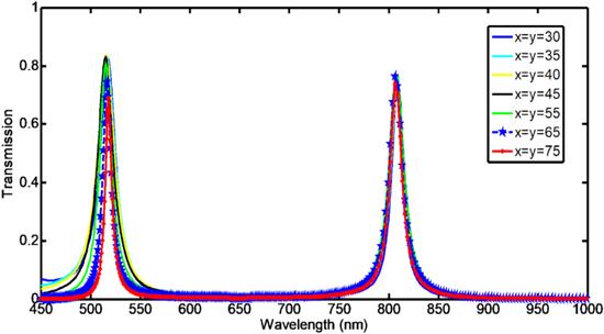
Figure 11. Transmission spectrum for different values of the triangle's edges (‘x' and ‘y'). |
6.3. Fabrication tolerances
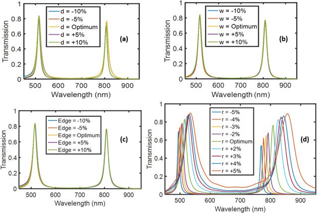
Such proposed designs are subject to a variety of geometric tolerances. In practice, different structural parameters can be deviated from the desirable values. In this study, the structure has been considered fabrication tolerances of the maximum $\pm 10 \% $ to their optimum values. The effects of deviations of the coupling distance between cavity and waveguide (d), the width of waveguide (w), the edges of the triangle (Edge), and the radius of resonator (r) have been investigated as illustrated in figure 12. As clearly seen in figure 12, deviation of the radius results in changes of transmission peaks and resonant wavelengths. Thus, precise fabrication is required related to the resonator. Furthermore, deviation of other parameters has no remarkable effect on transmission of the filter.
Figure 12. Deviation of different parameters on fabrication tolerances such as; (a) distance (b) width (c) edge (d) radius of the resonator. |
7. Results and comparisons
Finally, we have made a comparison between previous similar filters with our new designs. These new structures have beneficial characteristics such as tunable resonant wavelengths with sharp transmission peaks as presented in table 3. These proposed structures act as plasmonic band pass filters. The different parameters of the proposed filters and previous works with other topologies such as the number of modes (M), resonance wavelength ($\lambda $) and its maximum transmittance (${T}_{\max }$), and quality-factor (Q-factor) have been reported in table 3. The quality factor is another parameter which is important in the filters. It can be estimated from the below equation:
$ \begin{eqnarray}Q=\displaystyle \frac{{\lambda }_{0}}{{\rm{\Delta }}\lambda },\end{eqnarray}$
where ${\lambda }_{0}$ and ${\rm{\Delta }}\lambda $ are the peak wavelength and the bandwidth of the transmission spectrum, respectively. It is better to have a narrower spectral bandwidth or higher quality factor. Changing the geometry of the structure induces a higher peak transmission but broader bandwidth (smaller quality factor). Therefore, there is a tradeoff between the quality factor and the peak in transmission. In this paper, by changing the edges in the triangle, the quality factor has not been reduced significantly, but the better peak transmission is important in such filters, so that the reduction of the quality factor is ignorable. In comparison to the responses, the optimized filters with triangular-shaped adjunctions have higher transmission peaks than the same filters without triangular waveguides. Finally, the study on our new design focuses on peak transmission and two-mode structures. The transmittance in our new proposed filters can be up to 80%.Table 3. Different parameters of our new designed filters and previous topologies. |
| References | Year | M | $\lambda $(nm) | Maximum transmittance (%) | Q-factor |
|---|---|---|---|---|---|
| [58] | 2010 | 2 | 520 and 816 | 82.3 and 60 | 32.5 and 54.4 |
| [72] | 2011 | 2 | 655 and 1276 | 34 and 41 | 7.2 and 7.1 |
| [38] | 2011 | 2 | 583.5 and 1145 | 51 and 39 | 11.67 and 14.31 |
| [73] | 2013 | 2 | 829 and 1465 | 52.6 and 29.4 | 23.68 and 41.86 |
| [64] | 2013 | 2 | 517.3 and 803.4 | 74.3 and 45.7 | 64.66 and 114.7 |
| [74] | 2013 | 3 | 595 and 880 and 1550 | 11.85 and 55.45 and 88.66 | 9.15 and 11.89 and 25 |
| [75] | 2014 | 2 | 956 and 1550 | 80.7 and 72.3 | 25.83 and 28.18 |
| [76] | 2014 | 2 | 1110 and 1210 | 64.8 and 70.8 | 11.32 and 14 |
| [77] | 2015 | 1 | 940 | 89.8 | 23.5 |
| [78] | 2016 | 2 | 935 and 1626 | 75.3 and 58 | 21.25 and 35.21 |
| [79] | 2016 | 4 | 449 and 540 and 712 and 114 | 71.6 and 61 and 69 and 41 | 44.9 and 38.5 and 44.5 and 8.1 |
| Filter 1 | 2019 | 2 | 541 and 857 | 85 and 89.7 | 20.4 and 10.4 |
| Filter 2 | 2019 | 1 | 496 and 999 | 73 and 53 | 45.4 and 10.8 |
| Filter 3 | 2019 | 2 | 586 and 759 | 78 and 80 | 29.2 and 23 |
| Filter 4 | 2019 | 2 | 572 and 885 | 77 and 83 | 38.5 and 28.6 |
| Filter 5 | 2019 | 2 | 515 and 808 | 89 and 90 | 13.25 and 12.6 |
| Filter 6 | 2019 | 2 | 482 and 999 | 83 and 67 | 32.2 and 13.4 |
| Filter 7 | 2019 | 2 | 582 and 789 | 79 and 78 | 28.7 and 26.45 |
| Filter 8 | 2019 | 2 | 568 and 885 | 85 and 86 | 22.7 and 20.65 |
8. Conclusion
In summary, four improved band pass filters have been designed in this paper. The triangular-shaped-adjunctions in the proposed structures cause the increment of transmission. By varying the edges of triangle, the transmission will be increased. Each of these multi-mode filters have two modes with resonance wavelengths. The main goal is to obtain higher transmission so that the light will be passed through the waveguide. The shape of resonators and size of triangular-shaped adjunctions in waveguides play an important role in filters. The structures have been simulated using FDTD method. The optical plasmonic tunable band pass filter proposed here can be used in integrated circuits because of their small occupied area.