


1. Introduction
The increasing developments of III-Nitride semiconductors for promising new applications in the field of optoelectronics and energy applications can effectively reduce cost and energy consumption [1]. The III–V semiconductors and their alloys have burgeoning uses in photonics and optoelectronics. These materials are mostly used for high-frequency light emitting diodes (LEDs), optical detectors and laser diodes due to their high melting points, high thermal conductivity, large bulk modulus and wide band gaps. Gallium nitride (GaN) is among III-nitrides and has high chemical stability along with cost efficiency and energy. It has commercial usage in various applications including the UV photonics [2], UV optoelectronics [3], laser diodes, spin lasers [4], LEDs, piezoelectric sensors [5], ultraviolet or blue lasers, full color displays [6] and the high electron mobility transistors [7]. The zincblende (ZB) structure of GaN is more amenable than the wurtzite (WZ) structure and the ZB is preferred in research owing to its nano-technological applications. Remarkable investigations about the behavior of GaN under various dopants such as Zn, Mg, Cu has been studied to predict is potential uses [8–12]. Zn doping into GaN has been studied in the past as it has applications in electronic and optoelectronic devices [13–26]. It is revealed that in comparison to other dopants, the properties of Zn doped GaN are less well understood and there is an immense need to study its optical and electronic properties to find their potential applications in current technology. Moreover, due to universal rise in demand of solar energy, researchers across the globe are inspired to develop GaN based optoelectronic devices which have the ability to absorb incident light radiation in the UV and visible range. For this purpose, our Zn:GaN material seems suitable and show absorptivity in the UV region.
In the current study, we investigate the effects of Zn doping with different concertation on the structural, electronic, and optical properties of GaN using the first-principles calculations. The ground state energy, optimum volume, bulk modulus, and density of states (DOSs)are calculated and studied in detail. We find that Zn can be easily incorporated in GaN at different concentration under the N-rich condition due to lower formation energies. It has been observed that the lattice constant increases with increasing the Zn concentration in GaN due to smaller volume and larger atomic radius of Zn than Ga atoms. The Zn doping can significantly alter the semiconducting nature of GaN. No traces of spin-polarized ground state are observed in the doped GaN upon spin-polarized calculations [27]. We observed blueshift in absorption spectra along with increasing dopant concentrations and absorption trends shows prominent changes in the UV region because of quantum confinement effects. Refractive index and the dielectric constant increases with increasing Zn concentrations. Thus, our results furnish a route for the potential applications of zincblende GaN doped with Zn in the electronic and optical devices.
2. Computational method
All the calculations were performed with a supercell approach for investigating the structural, electronic and optical properties of GaN doped with Zn atoms. The supercell of GaN is constructed while extending unit cell by 2 times in the b and c directions i.e. $1\times 2\times 2$ (figure 1). The lattice parameter $a=b=c=4.51\,{\boldsymbol{\mathring{\rm{A}}}}$ with inclination angles $\alpha =\beta \,=\gamma =90^\circ $ and space group F-43m are used to simulate supercell [28]. The non-spin-polarized density functional calculations was performed in the framework of WIEN2K package [29]. We doped GaN with different Zn concentrations, namely, 6.25%, 12.50% and 18.70% in the supercell (table 1). The Ga-3d104s24p1, N-2s22p3 and Zn-3p63d104s2 states are considered the core states and the rest of states are assumed frozen. The generalized gradient approximation (GGA) based on Perdew–Burke–Ernzerhof was employed in order to approximate the exchange correlation potential [30, 31]. Then on-site coulomb interaction U (Hubbard parameter) was added to GGA functional. For strong correlation systems, the GGA + U results provide satisfaction and are compatible with the experimental findings [32]. Mostly, the Hubbard parameter value is opted from the justified values already reported in literature. We used the U = 0, 2, 4 and 6 eV values of Hubbard parameter [33] and study the effect of different U on the electronic and optical properties of Zn:GaN. The increasing effective values of U from 0 to 6 eV in GGA + U calculations influence the system and improved the lattice parameter in agreement with the experimental studies. We have applied different U values to the Zn 3d shells and found significant improvement in the electronic structure properties. Furthermore, to check the dynamical stability, we have calculated the phonon spectra as implemented in Phonopy code [34] within the framework of Wien2K code and are further confirmed with VASP package. Maximum value of expansion of wave function was used to be l = 10 and potential is spherically symmetric with constant value inside muffin-tin sphere. Gaussian smearing of 0.1 eV is used and self-consistent criterion is accompanied with charge, energy and force convergence of 10−2 C, 10−4 Ry and 1 mRy au−1 respectively. The RKmax value of 8 was chosen and the modified tetrahedron method in irreducible wedge is carried out using Brillouin zone integration [35]. After accomplishing the substitution, the iteration started until the convergence criterion is successfully obtained. k = 1000 points were used to perform calculations and relativistic effects were not incorporated in our study. Although, we have calculated all the electronic and optical properties for all U values (0, 2, 4, 6 eV) but for sake of avoiding complexity and for better readability, we have presented only selected data. In particular, we have reported results of lattice constants, bulk modulus, minimum energies, cohesive energies, and electronic properties.
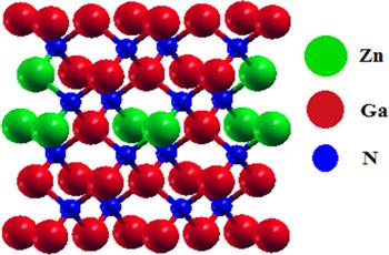
Figure 1. Supercell of Zn doped GaN for 18.70% Zn concentration. |
Table 1. Doping concentrations where Ga atoms are substituted with Zn atoms. |
| Case | 1 | 2 | 3 | 4 |
|---|---|---|---|---|
| Supercell | $1\times 2\times 2$ | $1\times 2\times 2$ | $1\times 2\times 2$ | $1\times 2\times 2$ |
| Atoms substituted | 0 | 1 | 2 | 3 |
| Doping concentrations | 0 | 6.25% | 12.50% | 18.70% |
3. Results and discussions
3.1. Structural properties
We studied structural properties of zincblende GaN doped with Zn at selected concentrations of 6.25%, 12.50% and 18.70% using Wien2K code. The structural optimization calculation is estimated by finding the minimum total energy using the Murnaghan’s equation of state [36, 37]
$\begin{eqnarray*}E\left(V\right)-E\left({V}_{0}\right)=\displaystyle \frac{{B}_{0}V}{{B}_{0}^{/}}\left[\displaystyle \frac{{\left({V}_{0}/V\right)}^{{B}_{0}^{/}}}{{B}_{0}^{/}-1}+1\right]-\displaystyle \frac{{B}_{0}{V}_{0}}{{B}_{0}^{/}-1},\end{eqnarray*}$
where V0 and ${B}_{0}$ are the equilibrium volume and bulk modulus respectively. Volume versus energy curves predict the stability of compound and are shown in figure 2. The calculated ground state minimum energies, bulk moduli, and equilibrium lattice parameters are listed in table 2 and compared to the reported theoretical and experimental data. Following the table 2, it is evident that by increasing the Zn concentration in GaN the lattice constant is increasing due to the smaller/larger volume/atomic radii of Zn than Ga. The calculated values of lattice constant are higher than the results of pure GaN discussed in findings [38–41]. The bulk moduli are compared to previous studies [42–44]. Since, we get correction in the electronic structure for U = 6 eV, so we have only presented structural optimization for this U value in order to filter current study from numerous figures, depicting the same meaning. Note that a similar increasing trend of lattice constant with increasing dopant concentration is already observed in doped III–V materials such as GaP and GaAs [45].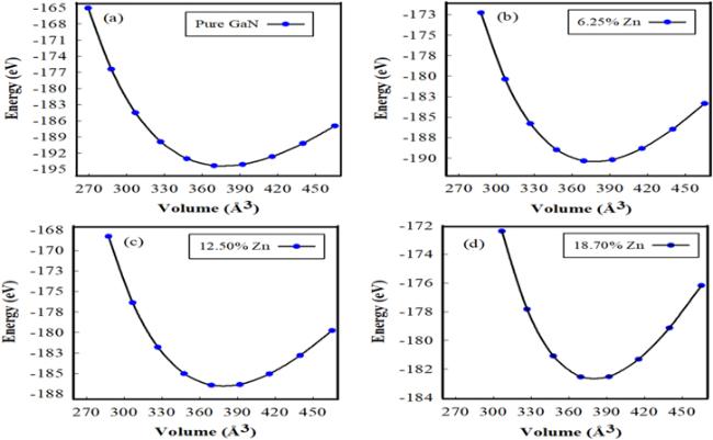
Figure 2. Structural optimization n curves of (a) pure GaN, and with Zn doping concentrations of (b) 6.25%, (c) 12.50% and (d) 18.70% for U = 6 eV. |
Table 2. Lattice constant (a), bulk modulus (B), minimum equilibrium energy (Emin), cohesive energy (ECohesive) and formation energies (Ef) of Zn doped GaN at different concentrations. |
| Ef (eV) | ||||||
|---|---|---|---|---|---|---|
| Concentration (%) | a (Å) | B(GPa) | Emin (eV) | ECohesive (eV) | Ga-rich | N-rich |
| 6.25 | U = 0; 4.80 | 215.75 | −170.66 | −11.28 | 2.26 | −3.32 |
| U = 2; 4.85 | 198.60 | −189.53 | −10.04 | 2.58 | −3.54 | |
| U = 4; 4.90 | 150.30 | −185.66 | −11.64 | 2.82 | −3.05 | |
| U = 6; 4.95 [48] | 190.75 [42, 44] | −190.44 | −13.49 [42, 43] | 2.23 [48] | −3.95 [48] | |
| 12.50 | U = 0; 4.98 | 250.08 | −177.00 | −14.06 | 3.65 | −5.78 |
| U = 2; 5.03 | 278.89 | −170.56 | −13.02 | 3.87 | −5.96 | |
| U = 4; 5.04 | 215.01 | −165.75 | −13.49 | 3.59 | −5.24 | |
| U = 6; 5.10 [49] | 175.08 [42, 44] | −186.42 | −11.50 [42, 43] | 4.46 | −4.67 | |
| 18.70 | U = 0; 5.18 | 167.47 | −190.54 | −11.09 | 3.99 | −2.32 |
| U = 2; 5.13 | 170.05 | −195.06 | −11.59 | 3.56 | −2.01 | |
| U = 4; 5.54 | 167.77 | −175.88 | −11.18 | 3.81 | −2.00 | |
| U = 6; 5.80 [49] | 170.54 [42, 44] | −182.54 | −10.70 [42, 43] | 7.46 | −1.20 | |
We have calculated the cohesive energies, in order to estimate the energy required to split each constituent atoms into its free atoms using the equation
$\begin{eqnarray*}{E}_{{\rm{cohesive}}}={E}_{{\rm{total}}}-\left({E}_{{\rm{Ga}}}+{E}_{{\rm{N}}}+{E}_{{\rm{GaN}}}\right),\end{eqnarray*}$
where Etotal, EGa, EN, and EGaN are the energies of GaN doped with Zn, energy of the Ga, N atom in their bulk form and the energy of the pure GaN, respectively. However, the calculated cohesive energies are slightly different than ECohesive of pure GaN [42, 43]. A review of cohesive energy indicates relative stabilities for dopant various concentrations as its values are emerging negative.
3.2. Phonon dispersion curves
The dynamical stability of the compound is very much needed for the practical synthesis of the materials and for this purpose, it is necessary to check the phonon vibrations. To determine the dynamical stability of Zn doped GaN material, we have calculated the phonon spectra using the density functional theory (DFT). Phonon modes present in the positive frequency range indicate the dynamical stability of the material for the synthesis [46]. The frequency dependent phonon spectra have been presented in figure 3. We have calculated phonon dispersions for three Zn concentrations 6.25%, 12.50% and 18.70%. Our results can be appreciated for the 6.25% and 18.70% Zn concentrations where phonon curves are well behaved (i.e. real). However, for the Zn 12.50% concentration, the existence of phonon spectra at imaginary frequencies directs instability of the material. Hence, Zn doping at 6.25% and 18.70% concentrations have better stability than at the 12.50% Zn concentration. Therefore because of stability, Zn doping at 6.25% and 18.70% concentrations will enhance the electronic and optical properties. Since, between these two concentrations, we get more corrections with effect of U = 6 eV so, we preferred to study its optical properties which have been discussed in section 3.5 . However, significant differences in phonon spectra emerges with the spectra presented in [47]. Hence, energetics calculations alone are not enough to predict the structure stability and phonon dispersions are essential.

Figure 3. Phonon dispersions of GaN with Zn concentrations of (a) 6.25%, (b) 12.50% and 18.70%. |
3.3. Formation energies
We dope Zn atom at the Ga-site in GaN. Note that it has been experimentally demonstrated that graphene can be doped by single dopant such as Pt, Co, and In [50]. To check whether the doping of Zn is energetically favorable in GaN, we have calculated the formation energy on the basis of chemical potential using the definition Ef = EZn@GaN $-$ EGaN + n($\mu $Ga $-\mu $Zn), where ${E}_{{\rm{Zn}}@{\rm{GaN}}}$ is the energy of the doped with n Zn atoms, ${E}_{{\rm{GaN}}}$ is the energy of the pristine GaN, n is the number of the doped Zn atoms, and ${\mu }_{{\rm{Ga}}}$ and ${\mu }_{{\rm{Zn}}}$ are the chemical potential of the elements Ga and Zn, respectively. To estimate the chemical potential, we have used the relation ${\mu }_{{\rm{GaN}}}\,={\mu }_{{\rm{Ga}}}+{\mu }_{{\rm{N}}},$ where ${\mu }_{{\rm{Ga}}}$ and ${\mu }_{{\rm{N}}}$ represent the chemical potentials of Ga and N, respectively. ${\mu }_{{\rm{GaN}}}$ can be considered as the total energy of pristine GaN per formula unit (EGaN). ${\mu }_{{\rm{Ga}}}$ for the Ga-rich environment is equal to ${{E}}_{{\rm{Ga}}},$ where ${{E}}_{{\rm{Ga}}}$ is the total energy of Ga per atom in the orthorhombic crystal structure. Thus, we can compute ${\mu }_{{\rm{N}}}$ for the Ga-rich environment from ${\mu }_{\mathrm{GaN}}-{\mu }_{\mathrm{Ga}}.$ For the N-rich condition, ${\mu }_{{\rm{N}}}$ is equal to ${E}_{{\rm{N}}},$ where ${E}_{{\rm{N}}}$ is the total energy of N per atom in the cubic crystal structure. Therefore, ${\mu }_{{\rm{Ga}}}$ can be calculated for the N-rich environment as ${\mu }_{\mathrm{GaN}}-{\mu }_{{\rm{N}}}.$ Table 2, tabulated the formation energies of nZn-doped GaN under the Ga- and N-rich conditions. From table 2, its can be seen that the formation energies under the N-rich condition for nZn-doped GaN are negative and lower than those under the Ga-rich condition, which means that Zn can be easily incorporated into GaN under the N-rich condition due to lower ${E}_{{\rm{f}}}$ [48]. Similar growth environment dependency has already been reported in the transition metal-doped SnSe2 [51] and SnS [52].
3.4. Density of states
The total density of states (TDOS) and partial density of states (PDOS) of Zn:GaN material have been presented in figures 4, 5. DOSs has been plotted in energy range −5 to 5 eV and contribution of Ga p-states, N p-states, and Zn d-states is clearly observed. Since, the results of PDOS and TDOS for pure GaN have been reported earlier [53, 54] so we did not repeat it in the current study. However, for pure GaN, the Ga pd- and N p-states are dominant with smaller contribution of Ga s- and N s-states. We observed significant improvement of states in the host GaN after Zn addition (figures 4, 5). The finite concentrations of impurity develops energy levels which helps in improving the electronic and optical properties of Zn:GaN. Figures 4, 5, shows a comparison among the electronic properties of DOSs for different values of Hubbard parameter (0, 2, 4, 6 eV). In figure 4 PDOS calculated for all the U values and we observed prominent role of Ga p- and N p-states [18]. But at the valence band maximum (VBmax), equal contribution of both p- and d-orbitals is noted for all concentration and the U values but for 18.70% Zn concentration, no orbital peaks are identified at VBmax for U = 0, 2 and 4 eV. For all concentration and U values, peaks comprising of N p-states are found at the Fermi level. On the other hand, application of different U values to the 3d orbitals of Zn atoms induces changes in d-levels compared to GGA. For better understanding of Hubbard corrections, we have only illustrated Zn 3d states to which various U values are applied as shown in the figures 5(d)–(f). We attest that addition of Hubbard parameter modified DOSs, i.e. significantly the position of d-states. A similar but slight shift of N 2p states can be observed. This shift may be understood as the coulomb energy treatment of electron–electron interaction of dopant 3d electrons [33]. It is pertinent to mention here that 3d states of dopant couple with the p-states of N and p–d hybridization is observed. The calculated TDOS also represent improvement for the U = 6 eV as compared to smaller values of U. A high accuracy of first principle calculations with implication of GGA + U method is presented in current study which is important for the future of materials systems with Zn (transition metal) 3d atom.
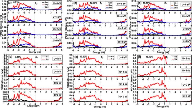
Figure 4. PDOS of (a) pure GaN, and with Zn doping concentrations of (b) 6.25%, (c) 12.50%, (d) 18.70% with implication of U = 0, 2, 4, 6 eV. The vertical dotted lines represent the Fermi level. |
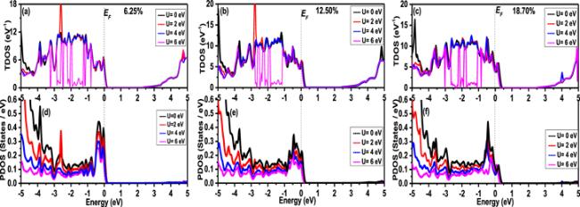
Figure 5. (a)–(c) TDOS and (d)–(f) PDOS of Zn 3d states for 6.25%, 12.50% and 18.70% Zn concentrations with implication of U = 0, 2, 4, 6 eV. |
3.5. Optical properties
Since optical properties are consistent with the change in electronic properties so we extend our DFT study to calculate the optical properties of Zn doped zincblende GaN. Optical properties are important to predict for any material as their information help us to suggest possible applications of materials in optical, optoelectronics, and photonic devices. Although, optical constants have been calculated for different U (0, 2, 4, 6 eV) values but we have only presented optical properties for U = 6 eV as electronic properties get corrected for U = 6 eV. Optical constants changes upon interaction with electromagnetic radiations. Investigation of the absorption coefficient ($\alpha $) of materials helps in materials selection to be used in optoelectronic devices. Absorption coefficient may be calculated using the formula [55]
$\begin{eqnarray*}\alpha \left(\omega \right)=\sqrt{2}{\left[\sqrt{{\varepsilon }_{{\rm{r}}}^{2}\left(\omega \right)+{\varepsilon }_{{\rm{i}}}^{2}\left(\omega \right)}-{\varepsilon }_{{\rm{r}}}\left(\omega \right)\right]}^{1/2},\end{eqnarray*}$
where $({\varepsilon }_{{\rm{r}}},\,{\varepsilon }_{{\rm{i}}})$ are real and imaginary part of the dielectric constant ($\varepsilon \left(\omega \right)={\varepsilon }_{{\rm{r}}}\left(\omega \right)+{\rm{i}}{\varepsilon }_{{\rm{i}}}\left(\omega \right)$). Figure 6(a), includes the absorption of pure GaN and Zn:GaN. For pure GaN, the maximum absorption is obtained at an energy value 9.68 eV (∼128 nm). The absorption edges of pure GaN are appeared at energies 3.91, 5.7, 6.6, 7.1, 7.8 and 9.68 eV. Our results are comparable to the reports [55–57]. In comparison to pure GaN, $\alpha \left(\omega \right)$ for various Zn concentrations show different trends and hence, the absorption edges occur at different energies. The absorption maxima for dopant various concentrations occur at energies; 9.68 eV ∼ 6.25%, 12.50% ∼9.86 eV and 10.07 eV ∼ 18.70%. A blueshift in the absorption spectrum is observed along with an increase in dopant contents. Absorption humps for various Zn concentrations are existing in low energy regions 0–2.6 eV and are shifted to higher frequencies upon increasing Zn concentrations. Shifting of these humps in low-frequency region may emerge due to quantum confinement effects [55] and may appear owing to excitations of electrons from the valence to conduction band. Pronounced variations in absorption spectra emerged with the effect of the existence of intermediate energy levels (3d) and are observed upon variations in dopant concentrations as seen in figure 5. It is all obvious that absorption spectra for Zn:GaN material is pronounced in the UV region whereas it decreased in NIR and visible region. Blueshift in absorption spectra is a signature of nanostructure formation of Zn:GaN material [55]. Moreover, by regulating the doping concentrations, a range of absorption can cover the entire solar spectrum and it broadens the scope of this material (Zn:GaN) to be effectively used in solar and photonic applications.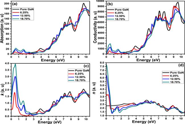
Figure 6. Optical spectra of Zn:GaN (a) absorption, (b) conductivity, (c) extinction coefficient and (d) refractive index with implication of U = 6 eV. |
Optical conductivity $\sigma \left(\omega \right)$ of pure GaN and Zn:GaN has been graphically demonstrated in figure 6(b). $\sigma \left(\omega \right)$ is calculated in term of the dielectric constant $\varepsilon \left(\omega \right)$ [55]
$\begin{eqnarray*}\sigma \left(\omega \right)=-{\rm{i}}\displaystyle \frac{\omega }{4\pi }\left|\varepsilon \left(\omega \right)-1\right|.\end{eqnarray*}$
The conductivity of pure GaN shows a constant rise after 2.3 eV and its maximum value is obtained at 9.57 eV. Conductivity humps are obtained at different energy values 3.90, 5.65, 6.64, 7.09, 7.7, 9.0 and 9.57 eV [55, 58]. The conductivity of Zn doped zincblende GaN system emerges due to the interaction of Zn atoms with N atoms as observed in figures 4, 5. However, conductivity maxima for various Zn concentrations are obtained at energy values; 6.25% ∼ 9.04 eV, 12.50% ∼ 9.2 eV and 18.70% ∼ 9.58 eV. Decrease in the conductivity in some energy regions may appear due to a decrease in absorption in those regions whereas emerging conductivity peaks may be explained in term of deep penetration of electromagnetic waves inside material and results increase in conductivity. Conductivity spectra are notably observed in the UV range and well-defined conductivity peaks as noted which are due to interband transitions.The extinction coefficient (k) is interrelated with the light absorption and is described as [55]
$\begin{eqnarray*}k=\displaystyle \frac{\alpha \lambda }{4\pi }.\end{eqnarray*}$
The k plots for pure GaN and Zn:GaN material have been demonstrated in figure 6(c) and plotted in energy range 0–10.5 eV. Extinction coefficient of pure GaN does not inspire from photon at lower energies but rises after 2.07 eV and kmax is achieved at energy value of 9.68 eV. In comparison to pure GaN, k values are appearing in low energy range for various Zn concentrations. k edges in low frequency range emerges due to fact that when light absorption increases then it extinct quickly and results in exhibiting higher k values. Extinction edges existing in energy region 0–1.30 eV are shifted to higher energies when dopant contents are increased. The k hump for lowest Zn concentration (6.25%) is not observed in range 1.3–2.57 eV. The extinction humps may be connected to electrons interband transitions from the valence to conduction band. The k values obtained in our study are in range 0–1.06 which are slightly higher than experimental value of k (0.26) obtained at 1.98 eV (621.1 nm) [56, 59]. The continuous rise and fall in k indicate property of material to absorb light at different energy values.Figure 6(d) depicts computed values of the refractive indices of the pure GaN and Zn:GaN system. Refractive index (n($\omega $)) is evaluated in term of real part of dielectric constant ${\varepsilon }_{r}$($\omega $) and changes effectively, when light penetrate inside the material. Variations in n are studied in energy range 0–10.5 eV. For the pure GaN, ${n}_{{\rm{\max }}}$ is observed at 230 nm (∼5.39 eV) while static value of refractive index (n(0)) is 2.3. Experimentally observed value of n for the pure GaN is 2.38 occurring at 632.8 nm corresponding to 1.95 eV [55, 60]. However, the static refractive indices values for various Zn concentrations are; 3.8%–6.25%, 6.3%–12.50% and 7.7%–18.70%. It is clear that n values computed in our computational (DFT + U) study are greater than the refractive index of the pure GaN. Increase in the n values with the effect of various Zn concentrations may appear due to slowing down of photons through successive interactions with electrons that exist in various concentrations (figures 4, 5).
The parameter of reflectivity ($R\left(\omega \right)$) gives information about the portion of radiation bouncing back in space. Reflectivity of Zn doped GaN system has been graphically manifested in figure 7(a). It is obtained using formula [55]
$\begin{eqnarray*}R\left(\omega \right)={\left[\displaystyle \frac{\sqrt{{\varepsilon }_{1}\left(\omega \right)+{\rm{i}}{\varepsilon }_{2}\left(\omega \right)}-1}{\sqrt{{\varepsilon }_{1}\left(\omega \right)+{\rm{i}}{\varepsilon }_{2}\left(\omega \right)}+1}\right]}^{2}.\end{eqnarray*}$
Variations in reflectivity suggest an increase and decrease in spectra in energy range 0–10.5 eV. Reflectivity peaks for pure GaN appears at energies; 2.26, 3.72, 5.59, 6.63, 7.1, 7.87 and 9.72 eV. However, reflectivity trends of Zn:GaN material are different than pure GaN such that reflectivity maxima are obtained in energy ranges; 6.25% ∼ 0–0.67 eV, 12.50% ∼ 0–0.9 eV and 18.70% ∼ 0–1.2 eV. Reflectivity maxima for various Zn concentrations are noticed at energies 6.25% ∼ 0.36 eV, 12.50% ∼ 0.03 eV and 18.70% ∼0.57 eV. Reflection occurs with the effect of collective oscillations of electrons and due to interband transitions. Moreover, multiple reflections within the material in low energy regions represent materials transparency for lower photon energies. Lower reflection in the high energy region enables the utilization of photons.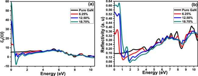
Figure 7. (a) ${\varepsilon }_{r}$ and (b) reflectivity of pure and doped GaN with various Zn concentrations with implication of U = 6 eV. |
Dielectric constant ($\varepsilon (\omega )$) of materials helps in predicting their optical applications. Probabilities of direct transitions and Kramers-Kronig dispersion relation yields real and imaginary part of dielectric constant [55]
$\begin{eqnarray*}{\varepsilon }_{i}\left(\omega \right)=\displaystyle \frac{4{\pi }^{2}}{{m}^{2}{\omega }^{2}}\displaystyle \displaystyle \sum _{V,C}\displaystyle {\int }_{{\rm{B}}{\rm{Z}}}\displaystyle \frac{2}{2{\pi }^{3}}{\left|{M}_{V,C}\left(k\right)\right|}^{2}\delta \left({E}_{C}^{k}-{E}_{V}^{k}-\hslash \omega \right){{\rm{d}}}^{3}k,\end{eqnarray*}$
$\begin{eqnarray*}{\varepsilon }_{{\rm{r}}}\left(\omega \right)=1+\displaystyle \frac{2}{\pi }{\rho }_{0}\displaystyle {\int }_{0}^{\infty }\displaystyle \frac{{\omega }^{/}{\varepsilon }_{{\rm{i}}}\left(\omega \right)}{{\omega }^{/2}-{\omega }^{2}}{\rm{d}}\omega .\end{eqnarray*}$
The real part of dielectric constant ${\varepsilon }_{r}\left(\omega \right)$ of pure GaN and Zn:GaN material has been shown in figure 7(b). Dielectric trends are meant for the response of the material to pass the electromagnetic field through it when different dopant concentrations are added to the host matrix. For pure GaN, the dielectric trait rises until the maximum dielectric value (8.8) is achieved at 5.3 eV. On the other side, dielectric response of Zn:GaN system shows sudden decreases at zero energy values and static value of dielectric constant corresponding to each concentration is; 14.64%–6.25%, 39.32%–12.50% and 58.78%–18.70%. Static dielectric constant ${\varepsilon }_{r}\left(0\right)$ for pure GaN (5.3) is smaller than Zn added GaN. The decrease in dielectric value with increasing energy (frequency) is because of polarization which cannot catch up with the varying electromagnetic fields in the high frequency (energy) range. The study of the dielectric constant suggests that at higher energy values (3.9–10.5 eV), the dielectric trends for Zn:GaN material are almost similar to that of pure GaN. ${\varepsilon }_{r}\left(\omega \right)$ has higher values in the low frequency region in comparison pure GaN and it is due to the existence of all type of polarization which may disappear upon a further increase in frequency. It is the reason that dielectric constant exhibit quite smaller values. However, for highest Zn concentration (18.70%), we observed negative dielectric constant values (in low frequency region). This negative trend of ${\varepsilon }_{r}\left(\omega \right)$ indicates the poor transmission through the material, thus exhibiting a considerable reflection. However, diverse range of transitions is responsible for further variations in ${\varepsilon }_{r}\left(\omega \right)$ at the higher energies.4. Conclusions
In this work, the DFT has been employed to investigate the structural, electronic, and optical properties of zinc doped zincblende GaN for the selected dopant concentrations (6.25%, 12.50%, 18.70%). We have used generalized gradient plus Hubbard (GGA + U) in the Wien2K code to deal with localized and correlated electrons. We substituted Ga atoms with Zn atoms in supercell ($1\times 2\times 2$) whereas the supercell is kept fixed for all concentrations. We found that doping of Zn in GaN at the Ga site suggests its easier incorporation under the N-rich condition and significantly alters the semiconducting properties of GaN. We have calculated the phonon dispersion curves and stability is revealed for the 6.25% and 18.70% Zn concentration while for the 12.50% Zn concentration, the instability in structure is observed. The addition of Hubbard values, U = 0, 2, 4, 6 eV are added to GGA and improvement in the electronic properties are observed for the U = 6 eV. We observed blueshift in absorption spectra along with increasing dopant concentrations and absorption trends show prominent changes in the UV region because of the quantum confinement effects. The prime contribution of cations (Zn) 3d states is revealed from the PDOS/TDOS results. The refractive indices and dielectric constants were increased with increasing dopant concentrations. Our results have resemblance with the reported literature works. Our DFT study will inspire experimentalists for preparing the Zn:GaN material which might have applications in the field of light harvesting devices including light displays, solar cells, spintronics, plasmonic devices, and sensors.