


1. Introduction
Two-dimensional materials have attracted great attention in the scientific community [1–5], researchers are exploring the unique electronic properties of single-layer and few-layer samples of these materials to develop new applications in the field of electronics, photonics, chemical sensing, catalysis, transport properties [6] and energy storage in the past few years [7–9]. On the other hand, the rapid development of graphene and the preparation of ultra-thin layers have triggered the exploration of other two-dimensional materials [10–13].
Graphene has been widely studied in many fields due to its excellent physical and chemical properties. Wehling et al [14] investigated the electronic properties of graphene upon water adsorption and studied the influence of the SiO2 substrate using density functional calculations, and they found that perfect suspended graphene is insensitive to H2O adsorbates while for graphene on a defective SiO2 substrate, they found a strongly different behavior. Feng et al [15] used density functional theory to calculate the adsorption energy, static charge and density of states, which proved that the optimization’s mechanism may lie in the effect of nitrogen and sulfur co-doping on the adsorption behavior of lithium atoms. Raad et al [16] used the first principles method based on the non-equilibrium Green’s function formalism to employ for the calculation of the device current in various environments, and their results show that there is little sensitivity toward H2O but it is very sensitive toward NH3 and NO2. Zhu et al [17] studied the reactions of ten air pollutants with non-defective and defective graphene to assess the safety of graphene using first principles, and they found pollutants other than ozone do not change the physical and chemical properties of non-defect graphene. Zhang et al [18] investigated how the Stone-Wales defect, the single vacancy, and the double vacancy affect the mechanical properties of graphene/aluminum composites, their results indicate that point defects enhance the interfacial bonding strength significantly and thus improve the mechanical properties of graphene/aluminum composites, especially the single vacancy defect. Jiang et al [19] have reported the computational realization of structural superlubricity for graphene/antimonene heterojunctions at the nanoscale using the first-principles method, the calculated results clearly demonstrate that structural superlubricity between graphene and antimonene monolayers could be achieved under the misaligned contacts. Zhang et al [20] investigated the adsorption of benzotriazole anion on defective graphene surface achieved the modification of N onto graphene, the results showed that the benzotriazole anion could absorbed on defective graphene rather on pristine graphene.
Although graphene has been studied to a considerable extent in the fields of interface reaction [23, 24], battery catalyst [21, 22], liquid penetration [25] and gas adsorption [26, 27]. There is a lack of research on the stability mechanism and optical properties of non-metal modified graphene. What is the structural stability of the doping system? What is the stability mechanism of the non-metal modified graphene? In this paper, the band structure, density of states, formation energy, charge density and optical properties of perfect graphene, B-, N-, Si-, S-doped graphene are designed based on the first-principles to reveal the mechanism of graphene modification by non-metallic elements, which will provide theoretical guidance for the application of optical properties for graphene. This publication is organized as follows, the calculation details are described in section 2 , the results and discussion are presented in section 3 . Finally, the conclusions are given in section 4 .
2. Calculation details
In this paper, all calculations are performed using a 4 × 4 × 1 graphene supercell with 32-atoms, and figure 1 shows four doping models of B-, N-, Si- and S-doped graphene supercell. As described above, all surface geometry is modeled as a periodic flat plate system, with a 20 Å vacuum between the surfaces sufficient to prevent interaction between periodic images. As shown in table 1, we compared the optimized results with other results and found that the super element size and calculation configuration we established are reasonable and reliable.
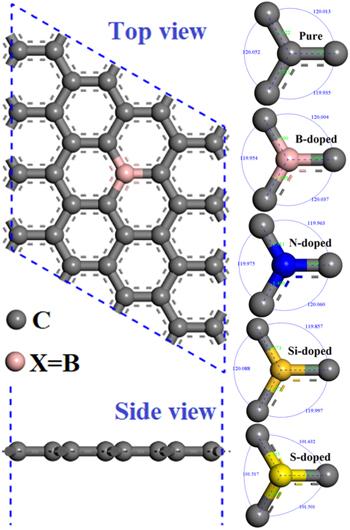
Figure 1. Top view and side view of intrinsic, B-doped, N-doped, Si-doped and S-doped graphene, the black, pink, blue, brown and yellow spheres represent C, B, N, Si and S atoms, respectively. |
Table 1. The calculation parameters and cell selection of graphene systems in comparison with other results. |
In our case of the calculation is performed via a first principles calculation as implemented in the Cambridge Sequential Total Energy Package (CASTEP) [28] Simulation package. The generalized gradient approximation (GGA) method of first-principles density functional theory (DFT) [29–31] is used to study the exchange correlation effect with Perdew–Burke–Ernzerhof (PBE) [32] functional. The main consideration is that GGA-PBE must take into account non-local and non-uniform effects when dealing with the exchange correlation between electrons. In all calculations, the cut-off energy of the plane wave is set to 450eV. Brillouin zone integrations are performed with the special k-point method over a Gamma centered 4 × 4 × 1 Monkhorst–Packmesh. Based on the crystal structure, density of states, electronic difference density, Mulliken population and the energy value of the system is calculated. These settings can achieve a higher iterative convergence accuracy (2×10⁻⁶ eV/atom), practice has proved that the calculation under this accuracy can ensure the accuracy and reliability of the graphene crystal structure. The force acting on each atom is not more than 0.05 eV/Å, and the internal stress is not more than 0.1 GPa. Drude damping is the specify the lifetime broadening for the Drude contribution [33], in the calculation details of this paper, 0.05 eV for Drude damping.
3. Results and discussion
Firstly, to compare the stability of different doping configurations, we calculate the formation energy of B-, N-, Si- and S-doped graphene systems. The calculation formula for formation energy is below:
$\begin{eqnarray}{\text{}}E({\rm{Form}})={\text{}}E({\rm{doped}})-{\text{}}E({\rm{pure}})+\mu ({\rm{C}})-\mu ({\rm{doped}}),\end{eqnarray}$
Among them, E(doped) is the total energy of the doped system, E(pure) is the total energy of intrinsic graphene, μ(C) is the chemical potential of a single C atom, and μ(doped) is the chemical potential of a single doped atom (B, N, Si, S).3.1. Structural stability of different doping systems
The doped graphene model is completed on a 4 × 4 periodic graphene supercell. This supercell contains 32 atoms and is constructed by replacing one of the C atoms, so the periodicity of perfect graphene is destroyed, as shown in figure 1. From figure 1 we can see that in the system doped with B, N, Si, and S, the C-C bond structure has undergone a certain degree of change, including the bond length and bond angle. The bond lengths and angles near the doping atoms (B, N, Si, S) vary significantly. Table 2 shows the bond length changes between the doping atoms (B, N, Si, S) and the three adjacent C atoms. From the changing of bond length, it can be seen that the bond length of B-, N-, Si-, S-doped graphene systems have a certain degree of change compared with the C-C bond length in perfect graphene (1.421 Å). The S-C bond is the longest (1.73 Å), followed by the Si-C bond (1.67 Å), and the B-C bond (1.49 Å) is the middle one. To sum up, the doped bond lengths in the B-doped, Si-doped and S-doped systems all increase at a certain level, but only the bond length of the N-C bond in N-doped system decreases (1.41 Å).
Table 2. The calculated different configuration, C-X distance [d(C-X)], bond angle (C-X-C), charge transfer(Q), formation energy, atomic radius, radius difference, bond order. |
| Configuration | d(C-X)/Å | A(C-X-C)/° | Q(e) | Formation energy (eV) | Radius of the doping atom/Å | Radius difference(%) | Bond order |
|---|---|---|---|---|---|---|---|
| Pure graphene | 1.42 | 120.00 | — | — | 0.91 | — | — |
| B-doped graphene | 1.49 | 120.03 | 0.58 | 3.62 | 1.17 | 0.28 | 9 |
| N-doped graphene | 1.41 | 119.96 | −0.26 | 1.83 | 0.75 | 0.17 | 9 |
| Si-doped graphene | 1.67 | 119.86 | 1.83 | 8.02 | 1.46 | 0.60 | 8 |
| S-doped graphene | 1.73 | 101.63 | 0.81 | 8.79 | 1.09 | 0.19 | 6 |
At the same time, we calculated the formation energy of each doping system according to formula 1. The formation energies of the four doping models of B, N, Si, and S are shown in figure 2. As we can see in figure 2 that the order of formation energies is: N, B, Si, S, which indicates that the doping of the N atom is lower than that of the B, Si, and S atoms. It can also be seen from table 2 that the N-C bond length is significantly smaller than B-C, Si-C, and S-C. The N-C bond length is slightly smaller than the C-C bond length and is almost equal. We have calculated the bond order of the graphene doped with four non-metallic elements. As shown in table 2, it is found that the bond order of N-, B-, Si-, S-doped graphene decreases in order, so the order of stability is: N-, B-, Si-, S-doped graphene, which are consistent with our calculation results of the formation energy. Through comparison, it is found that compared with B, Si, and S atom doped systems, an N atom has a smaller atomic difference and a smaller lattice distortion, which results in a smaller formation energy. Our computational simulation results are in agreement with those of other experimental researchers [36].
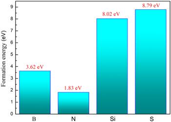
Figure 2. The formation energy of B-, N-, Si-, S-doped graphene. |
3.2. Electronic structure of different doping systems
In order to better understand the mechanism of interaction between the doped atoms (B, N, Si, S) and graphene, we further calculated the band structure, density of states and charge density of the doped system. As shown in figure 3, we performed a systematic calculation of the band structure for unit cell of intrinsic graphene, the supercell of intrinsic graphene and B-, N-, Si- and S-doped graphene. From figures 3(a) and (b), we can see that the unit cell of intrinsic graphene and supercell of intrinsic graphene are all zero band gap semiconductor material. The results show that the expansion behavior of graphene does not have much effect on its band structure. It can be seen from figures 3(c) and (e) that the Fermi level has moved down due to the introduction of B atoms and Si atoms, which is because the B atom has only three valence electrons, one electron less than the C atom, and it is a typical p-type doping. It can be seen from figure 3(d) that the Fermi level moves up due to the presence of N atoms. This is because N atoms have five valence electrons, one more electron than C atoms, which is a typical n-type doping. We can seen from figure 3(e) that the introduction of an Si atom leads to the generation of impurity bands near the Fermi level. As shown in figure 4, we have systematically calculated the total density of states and atomic partial density of states of the perfect graphene and B-, N-, Si- and S-doped graphene. From figure 4(b), we can see that the perfect graphene exhibits a zero band gap semiconductor property, which is consistent with our previous calculation results of the band structure. We can observe from figures 4(c) and (e) that in the B- and Si-doped graphene systems, the total density of states is near the Fermi level, and the top of the valence band crosses the Fermi level, showing a p-type. The characteristics of doping are consistent with the calculation results of the band structure results. It can be seen from the partial density of states of the B atom and its neighboring C atom that B atoms and C atoms have a tendency to interact with each other in the valence band, as shown in figure 4(c). The sharp peaks appear, indicating that the B-doped system has formed a strong B-C covalent bond. It can be observed from figure 4(e) that the bottom part of the conduction band has crossed the Fermi level, making the doping system exhibit n-type doping characteristics, which is the result of the coupling effect between the p orbital of the N atom and the p orbital of the C atom. In figure 4(f), it can be seen that the total density of states has a sharp peak at the Fermi level, indicating the existence of an impurity band, which is consistent with the previous calculation of the band structure.
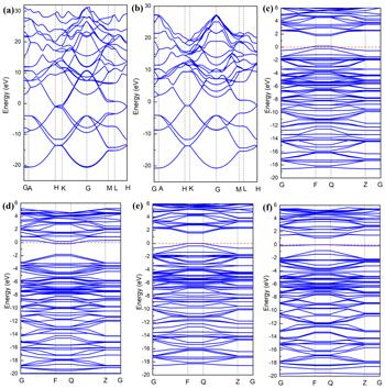
Figure 3. Band structure of (a) unit cell of intrinsic graphene, (b) supercell of intrinsic graphene, (c) B-, (d) N-, (e) Si- and (f) S-doped graphene. |
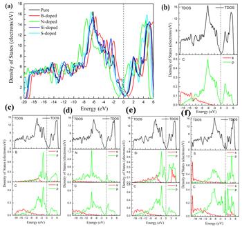
Figure 4. Density of states and partial density of states of (a) intrinsic, (b) B-, (c) N-, (d) Si- and (e) S-doped graphene. |
To visually see how the doped atoms (B, N, Si, S) interact with graphene, we further calculated the Mulliken charge changes of the doped atom system, as shown in table 2. It can be seen from table 2 that the three B, Si, and S atoms lose their electrons and show a positive charge, which are respectively 0.58 e, 1.83 e, and 0.81 e, showing the characteristics of easy access to electrons. However, the N atom gains electrons and shows electronegativity (-0.26 e), showing the characteristic of easily losing electrons.
In order to observe the modification of graphene by B, N, Si, and S more intuitively, we calculated the electron density and charge density difference of the perfect graphene and the B-, N-, Si- and S-doped graphene system, respectively, as shown in figure 5. The electron density and charge density difference of the perfect graphene show a uniform distribution, indicating that the electrons gain and loss between C and C are relatively uniform in the perfect graphene. From figures 5(b)–(e), it can be seen that the dopant atoms B, Si, and S are surrounded by the blue region, respectively, indicating the loss of electrons, while the N atom is surrounded by the red region, and the results are consistent with the analysis in table 2.
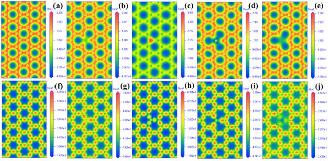
Figure 5. Electron density of (a) intrinsic, (b) B-, (c) N-, (d) Si- and (e) S-doped graphene, charge density difference of (f) intrinsic, (g) B-, (h) N-, (i) Si- and (j) S-doped graphene. |
3.3. The surface optical properties of different doping systems
The doped atoms on the material surface changes the optical properties of the material. The dielectric function is the responsiveness of a material to react to visible light. The dielectric function can be characterized as follows:
$\begin{eqnarray}{\varepsilon }_{}(\omega )={\varepsilon }_{1}(\omega )+{\rm{i}}{\varepsilon }_{2}(\omega ),\end{eqnarray}$
the ϵ1(ω) represents the real part of the function, the ϵ1(ω) is the imaginary part. We conducted a systematic study on the optical properties of different configurations, which are plotted in figures 6(a)–(d). Among them, black, red, cyan, blue and green represent intrinsic, B-doped, N-doped, Si-doped and S-doped graphene respectively. It can be seen from figure 6(c) that the absorption coefficient of intrinsic graphene increases continuously in the 1.6 eV–3.1 eV interval, and the absorption peak reaches the highest value at 3.1 eV, and the absorption coefficient is 3.0 × 104 cm−1. From figure 6, we can see that in the visible light region, compared with the intrinsic graphene system, the absorption spectrum of the Si-, S-doped graphene system have an upward trend, while the absorption spectrum of the B-, N-doped graphene system has a downward trend. It is found that the sensitivity to light in the visible light region is ranked as follows: S-doped> Si-doped> pure > B-doped > N-doped. Our research results provide theoretical guidance for the research of graphene-based optical materials.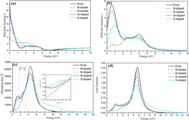
Figure 6. The real spectra of optical dielectric function (a), the imaginary spectra of optical dielectric function (b), absorption spectrum (c) and loss function (d) of intrinsic, B-, N-, Si- and S-doped graphene, respectively. |
4. Conclusions
In this paper, using the first-principles method based on density functional theory we have studied the electronic structure and stability of the intrinsic, B-, N-, Si-, S-doped graphene. The band structure, density of states, formation energy, charge density and optical properties of perfect graphene, B-, N-, Si-, S-doped graphene were investigated in detail. The results show that the ease of doping for the four non-metal atoms is N, B, Si, S in order. In addition, the B and Si-doped graphene system is a typical p-type doping, and the N-doped graphene system is an n-type doping. The doped S atom makes the system have impurity bands. The research results also show that after four non-metallic atoms doping, B, Si, and S lose their electrons to show positiveness and have the characteristics of easy access to electrons, while N atoms get electrons to show electronegativity and show that they are easy to lose electrons. The results of its optical properties show that the sensitivity to light in the visible light region is ranked as follows: S-doped> Si-doped> pure > B-doped > N-doped. Our research results provide a theoretical basis for further research on the stability and electronic properties of graphene-based materials.