


1. Introduction
Surface plasmons (SPs) are surface electromagnetic waves that exist at the interface between metal and dielectric, and they include localized surface plasmons (LSPs) and surface plasmon polaritions (SPPs) [1, 2]. LSPs are confined to the vicinity of metal nanostructures, while SPPs are localized near the metal-medium interface and spread along it [3–5]. Importantly, the SPPs can surmount traditional optical diffraction limits and manipulate light at the sub-wavelength range [6]. Accordingly, SPPs play a vital role in various plasmonic devices, such as filters [7], optical switches [8–11], absorbers [12–14], polarizers [15], slow-light devices [16], modulators [17] and others. However, the non-dynamic adjustability and the large ohmic loss of the metal-based SPPs severely restrict the development of SPPs-based devices. Fortunately, graphene can prominently overcome the above shortcomings and become a good metal substitute for the propagation of SPPs.
Graphene, a two-dimensional carbon nanomaterial with excellent dynamic regulation characteristics, has become a hotspot in research due to its high carrier mobility [18], electrical tunability [19–21] and low transmission loss [22]. It has important applications in the fields of modulators [23, 24], sensors [25, 26], photodetectors [27, 28], and so on. In addition, graphene shows metal-like dielectric properties in terahertz band, which enables graphene to propagate the transverse magnetic mode of SPPs wave. Although the optical properties of graphene-based SPPs are similar to that of metal-based SPPs in many ways, there are many advantages that metal does not have. For example, the Fermi energy of graphene can be easily regulated by adjusting the bias voltage, so the spectral characteristics based on the graphene structures can be dynamically modulated without changing the structural parameters. Based on the above advantages, the applications and explorations of graphene in various functional devices are booming.
The plasma-induced transparency (PIT) is an optical abnormal phenomenon produced by the destructive interference between the resonant modes of SPPs. In the meanwhile, it is a plasmonic analogy of classical electromagnetically induced transparency (EIT) [29]. Compared with EIT, PIT is not restricted by the stable optical pumping source, gaseous medium, extremely low-temperature environment and other harsh experimental conditions [30]. The PIT phenomenon has been observed in both graphene and metal, but due to the great advantage of graphene’s dynamic modulation, it is mainly used in graphene materials. Normally, the single-PIT comes from the interaction between a bright mode and a dark mode [31, 32] or two bright modes [33, 34]. The bright mode can be easily excited by the incident light and produces opaque valleys which are called Lorentz lines in the transmission spectrum, whereas the dark mode can not be directly excited by the incident light, but it can be excited by the light field which is generated by the interaction between the incident light and the bright mode. The resonance of the dark mode and the bright mode at certain frequency points leads to the formation of two transmission valleys and a PIT window. In addition to single PIT, the dual-PIT has been realized in the single-layer and multi-layer graphene structure. The single-PIT and dual-PIT have been widely used in absorbers, modulators and so on. However, up to date, there are few studies on the triple-PIT with an optical-switching function which is based on the multilayer graphene structure.
In this paper, we propose a bilayer graphene periodic structure composed of upper-layer double graphene ribbons and lower-layer double graphene rings to realize tunable triple-PIT. The simulated results by using of the finite-difference time-domain (FDTD) [35] are consistent with the theoretically calculated results via coupled mode theory (CMT), which represents the correctness of our theoretical analysis [36]. Unexpectedly, by adjusting the Fermi levels of graphene, we realized a penta-frequency asynchronous and a double-frequency or triple-frequency synchronous optical switches. The maximum modulation depth (MD) and the minimum insertion loss (IL) of the switches are 99.97% and 0.33 dB, respectively. Additionally, our structure shows excellent slow light characteristics with a maximum time delay up to 0.848 ps. Therefore, these high-performance characteristics provide a theoretical guide for the study of multi-frequency optical switches and excellent slow-light devices.
2. Structure and theoretical model
The structure shown in figure 1(a) is a metamaterial unit composed of the upper layer graphene (ULG), the interlayer with a silicon material, the lower layer graphene (LLG) and the substrate silicon. Silicon is a common semiconductor material with weak electrical conductivity and can be easily processed using standard lithography technologies in experiment [37]. The red parts in figure 1 represent the ULG and LLG which are two identical graphene ribbons and two concentric rings with different sizes, respectively. The structural plane diagrams of ULG and LLG are shown in figure 1(b). Their geometric parameters are as follows: Lx =4 μm, Ly = 4 μm, L1 = 1.49 μm, L2 = 2.02 μm (the outer diameter of big graphene ring (BGR)), L3 = 1.62 μm (the inner diameter of BGR), L4 = 1.02 μm (the outer diameter of small graphene ring (SGR)), L5 = 0.62 μm (the inner diameter of SGR), d1 = 0.2 μm, d2 = 0.3 μm. Triple-PIT phenomenon occurs when the whole structure (WS) is illuminated perpendicularly by an x-polarized plane wave which is incident along the negative direction of the z-axis. At this time, the intensity of the plane wave is very weak, and the nonlinear effect of graphene has almost no effect, so it can be ignored. The conductivity σg of the monolayer graphene consists of intraband electron photon scattering and direct interband photon transition. In the low terahertz band, direct interband photon transition can be ignored owing to the condition EF ≥ kBT = 25.85 meV [38]. Therefore, the conductivity of the single-layer graphene can be expressed as [39]:
$\begin{eqnarray}{\sigma }_{g}=\displaystyle \frac{{\rm{i}}{e}^{2}{E}_{F}}{\pi {{\hslash }}^{2}\omega +{\rm{i}}{\tau }^{-1}},\end{eqnarray}$
where e, EF, ω,ℏ, and τ are the electronic charge, the Fermi level of graphene, the angular frequency of incident light, the reduced Planck constant and the carrier relaxation time, respectively. Here, τ = μEF/(e${{V}_{F}}^{2}$), μ is the carrier mobility, VF ≈ c/300 is the Fermi velocity, c is the speed of light. The experimental results show that the carrier mobility μ of graphene can reach 4 m2 (V−1 s−1) at room temperature [40]. Considering the actual operation situation, we fix μ and VF to 3.5 m2 (V−1 s−1) and 106 m (s−1), respectively.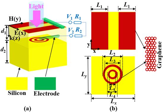
Figure 1. (a) Structure diagram of double layer graphene metamaterial. (b) Schematic of ULG and LLG. |
Due to the ULG is between the medium air and the substrate silicon, the dispersion relation can be solved by Maxwell equations and electromagnetic field boundary conditions. It can be expressed as [41]:
$\begin{eqnarray}\displaystyle \frac{{\varepsilon }_{\mathrm{si}}}{\sqrt{{\beta }^{2}-{\varepsilon }_{\mathrm{si}}{k}_{0}^{2}}}+\displaystyle \frac{{\varepsilon }_{\mathrm{air}}}{\sqrt{{\beta }^{2}-{\varepsilon }_{\mathrm{air}}{k}_{0}^{2}}}=-\displaystyle \frac{{\rm{i}}{\sigma }_{g}}{\omega {\varepsilon }_{0}}.\end{eqnarray}$
Since the media above and below LLG are silicon, the dispersion relation is expressed as [4]: $\begin{eqnarray}\displaystyle \frac{{\varepsilon }_{\mathrm{si}}}{\sqrt{{\beta }^{2}-{\varepsilon }_{\mathrm{si}}{k}_{0}^{2}}}+\displaystyle \frac{{\varepsilon }_{\mathrm{si}}}{\sqrt{{\beta }^{2}-{\varepsilon }_{\mathrm{si}}{k}_{0}^{2}}}=-\displaystyle \frac{{\rm{i}}{\sigma }_{g}}{\omega {\varepsilon }_{0}}.\end{eqnarray}$
Here, ϵsi = 11.9 is the relative permittivity of silicon, ϵair = 1 is the relative permittivity of air, β is the propagation constant, k0 is the wave vector of incident light, and ϵ0 is the dielectric constant of vacuum.The electric circuit used to adjust the Fermi levels of the upper and lower graphene is schematically drawn in figure 1(a). It can be seen that the gate voltages V1 and V2 are contacted to ULG and LLG by two electrodes, respectively. The applied voltage can push electrons into the hole of graphene and then regulate the carrier concentration of graphene, promoting a change value of the Fermi energy of graphene [42]. Thus, the Fermi levels of ULG and LLG can be respectively changed by adjusting the gate voltages V1 and V2 in figure 1(a). The electrodes in the device are theoretical schematic regulation between Fermi energy and applied voltage. The relationship between the Fermi levels of ULG and LLG and the gate voltages can be respectively expressed as follows [43]:
$\begin{eqnarray}\begin{array}{rcl}{E}_{F}(\mathrm{ULG}) & = & {\hslash }{V}_{F}\sqrt{\displaystyle \frac{\pi {\varepsilon }_{0}{\varepsilon }_{\mathrm{si}}{V}_{1}}{{d}_{1}e}},\\ {E}_{F}(\mathrm{LLG}) & = & {\hslash }{V}_{F}\sqrt{\displaystyle \frac{\pi {\varepsilon }_{0}{\varepsilon }_{\mathrm{si}}{V}_{2}}{{d}_{1}e}}.\end{array}\end{eqnarray}$
The transmission spectra of four graphene metamaterial structures are shown in figure 2(e). It can be seen that when the ULG (figure 2(a)), BGR (figure 2(b)) and SGR (figure 2(c)) exist alone, they are all bright radiation modes within a certain frequency range, when they make up the WS, the triple-PIT phenomenon will appear. In order to further analyze the formation of the triple-PIT phenomenon, we divide figure 2(e) into four individual frequency regions: (1), (2), (3), (4). At the same time, the resonant dips of the WS’s transmission spectrum are named dip1, dip2, dip3 and dip4 (from left to right). The corresponding frequencies of these four dips are f1 = 1.509 THz, f2 = 3.076 THz, f3 = 4.108 THz and f4 = 5.397 THz, respectively. In addition, the distributions of electric field intensity corresponding to the four frequencies are showed in figures 2(f)–(i).
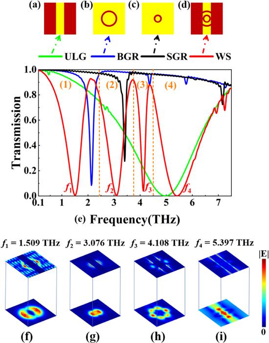
Figure 2. (a)–(d) Schematic diagrams of three separate structures and the whole structure. (e) Transmission spectra of four graphene structures. (The Fermi level is set to 1.0 eV) (f)–(i) Distributions of electric field intensity at the corresponding four frequency points. |
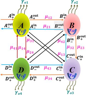
Figure 3. Schematic diagram of coupled mode theory. |
In the first frequency region (1) in figure 2(e), ULG and SGR act as two dark modes and BGR acts as a bright mode. As displayed in figure 2(f), the light field energy is mainly located around BGR and ULG. Namely, ULG is excited by the coupled light field between BGR and incident light, so the formation of dip1 is mainly contributed to BGR and ULG. In the second frequency region (2), in this case, SGR acts as a bright mode, while BGR and ULG act as two dark modes. The electric field energy is mainly concentrated on SGR according to figure 2(g), so the two dark modes BGR and ULG were not excited, indicating that the formation of dip2 is mainly attributed to SGR. In the third frequency region (3), ULG serves as the bright mode, while BGR and SGR serve as the dark mode. The interaction between them forms dip3. It can be found from figure 2(h) that the electric field intensity is mainly distributed on the BGR and UGR. Accordingly, the ULG acting as a bright mode is directly excited, while the BGR serving as a dark mode is excited indirectly by the coupled light field between the incident light and the ULG. Therefore, the interaction between the bright mode ULG and the dark mode BGR forms the dip3. In the fourth frequency region (4), ULG still acts as the bright mode, BGR and SGR act as the dark modes, too. It can be seen from the electric field diagram in figure 2(i) that the light field energy is located around the BGR, SGR and the ULG. It can be concluded that ULG as bright mode is directly excited by incident light, and BGR and SGR as two dark modes are indirectly excited. Therefore, the formation of dip4 is mainly caused by the interaction among the three structures. We can draw the conclusion that the interaction between those models caused by ULG, BGR and SGR will form the obvious triple-PIT phenomenon.
Next, CMT [37, 44] is used to fit the transmission spectra which are obtained by FDTD simulations and to explain the coupling effect. In figure 3, A, B, C and D represent four hypothetical resonator modes, whose amplitudes are a, b, c and d, respectively. The superscript ‘in/out’ and the subcript ‘±’ of ${A}_{\pm }^{\mathrm{in}/\mathrm{out}}$, ${B}_{\pm }^{\mathrm{in}/\mathrm{out}}$, ${C}_{\pm }^{\mathrm{in}/\mathrm{out}}$ and ${D}_{\pm }^{\mathrm{in}/\mathrm{out}}$ represent input or output plasmon waves and the positive or negative propagating direction of plasmon waves, respectively. μmn (m, n = 1, 2, 3, 4, m ≠ n) is the mutual coupling coefficient among the four radiation modes. γin and γon denote the internal and external loss coefficients of the four hypothetical resonators, respectively. The coupling relationship between the four resonators can be expressed as [43]:1 ), (2 ) and (3 ). Qon is the external loss quality factor of the nth resonant mode. Qin and Qon are satisfied by the following equation (1 )/Qtn = 1/Qin + 1/Qon. Here, Qtn is the total quality factor of the nth resonant mode which can be obtained by the ratio of the resonant frequency to 3 dB bandwidth: Qtn = fn/Δfn. fn and Δfn are the resonant frequency and the full width at half maximum of the nth resonant mode, respectively. According to the conservation of energy, the relationships among the four coupled modes are as follows:
$\begin{eqnarray}\begin{array}{l}\left(\begin{array}{cccc}{\gamma }_{1} & -{\rm{i}}{\mu }_{12} & -{\rm{i}}{\mu }_{13} & -{\rm{i}}{\mu }_{14}\\ -{\rm{i}}{\mu }_{21} & {\gamma }_{2} & -{\rm{i}}{\mu }_{23} & -{\rm{i}}{\mu }_{24}\\ -{\rm{i}}{\mu }_{31} & -{\rm{i}}{\mu }_{32} & {\gamma }_{3} & -{\rm{i}}{\mu }_{34}\\ -{\rm{i}}{\mu }_{41} & -{\rm{i}}{\mu }_{42} & -{\rm{i}}{\mu }_{43} & {\gamma }_{4}\end{array}\right)\cdot \left(\begin{array}{c}a\\ b\\ c\\ d\end{array}\right)\\ \quad =\left(\begin{array}{cccc}-{\gamma }_{o1}^{1/2} & 0 & 0 & 0\\ 0 & -{\gamma }_{o2}^{1/2} & 0 & 0\\ 0 & 0 & -{\gamma }_{o3}^{1/2} & 0\\ 0 & 0 & 0 & -{\gamma }_{o4}^{1/2}\end{array}\right)\cdot \left(\begin{array}{c}{A}_{+}^{\mathrm{in}}+{A}_{-}^{\mathrm{in}}\\ {B}_{+}^{\mathrm{in}}+{B}_{-}^{\mathrm{in}}\\ {C}_{+}^{\mathrm{in}}+{C}_{-}^{\mathrm{in}}\\ {D}_{+}^{\mathrm{in}}+{D}_{-}^{\mathrm{in}}\end{array}\right).\end{array}\end{eqnarray}$
γn = iω − iωn − γin − γon, where i, ωn and ω are the imaginary unit, the nth resonant angular frequency and the angular frequency of incident light, respectively. Here, ωn is calculated by ωn = 2πfn, fn represents f1, f2, f3 and f4 in figure 2(a), γin = ωn/(2Qin) and γon = ωn/(2Qon). Qin is the internal loss quality factor of the nth resonant mode, which can be expressed as Qin = Re(neff)/Im(neff). The effective refractive index is neff = β/k0. The relation between β and ω can be obtained from equations ( $\begin{eqnarray}{D}_{-}^{\mathrm{in}}=0,\end{eqnarray}$
$\begin{eqnarray}{B}_{+}^{\mathrm{in}}={A}_{+}^{\mathrm{out}}\cdot {{\rm{e}}}^{{\rm{i}}{\varphi }_{1}},{A}_{-}^{\mathrm{in}}={B}_{-}^{\mathrm{out}}\cdot {{\rm{e}}}^{{\rm{i}}{\varphi }_{1}},\end{eqnarray}$
$\begin{eqnarray}{C}_{+}^{\mathrm{in}}={B}_{+}^{\mathrm{out}}\cdot {{\rm{e}}}^{{\rm{i}}{\varphi }_{2}},{B}_{-}^{\mathrm{in}}={C}_{-}^{\mathrm{out}}\cdot {{\rm{e}}}^{{\rm{i}}{\varphi }_{2}},\end{eqnarray}$
$\begin{eqnarray}{D}_{+}^{\mathrm{in}}={C}_{+}^{\mathrm{out}}\cdot {{\rm{e}}}^{{\rm{i}}{\varphi }_{3}},{C}_{-}^{\mathrm{in}}={D}_{-}^{\mathrm{out}}\cdot {{\rm{e}}}^{{\rm{i}}{\varphi }_{3}},\end{eqnarray}$
$\begin{eqnarray}{A}_{+}^{\mathrm{out}}={A}_{+}^{\mathrm{in}}-{\gamma }_{o1}^{1/2}\cdot a,{A}_{-}^{\mathrm{out}}={A}_{-}^{\mathrm{in}}-{\gamma }_{o1}^{1/2}\cdot a,\end{eqnarray}$
$\begin{eqnarray}{B}_{+}^{\mathrm{out}}={B}_{+}^{\mathrm{in}}-{\gamma }_{o2}^{1/2}\cdot b,{B}_{-}^{\mathrm{out}}={B}_{-}^{\mathrm{in}}-{\gamma }_{o2}^{1/2}\cdot b,\end{eqnarray}$
$\begin{eqnarray}{C}_{+}^{\mathrm{out}}={C}_{+}^{\mathrm{in}}-{\gamma }_{o3}^{1/2}\cdot c,{C}_{-}^{\mathrm{out}}={C}_{-}^{\mathrm{in}}-{\gamma }_{o3}^{1/2}\cdot c,\end{eqnarray}$
$\begin{eqnarray}{D}_{+}^{\mathrm{out}}={D}_{+}^{\mathrm{in}}-{\gamma }_{o4}^{1/2}\cdot d,{D}_{-}^{\mathrm{out}}={D}_{-}^{\mathrm{in}}-{\gamma }_{o4}^{1/2}\cdot d,\end{eqnarray}$
where φ1, φ2 and φ3 refer to the phase difference between resonators A and B, B and C, C and D, φn = Re(β)dn. (n = 1, 2, 3).By combining the above formulas, the transmission coefficient of the system can be obtained by:
$\begin{eqnarray}\begin{array}{rcl}t & = & \displaystyle \frac{{D}_{+}^{\mathrm{out}}}{{A}_{+}^{\mathrm{in}}}={{\rm{e}}}^{{\rm{i}}({\varphi }_{1}+{\varphi }_{2}+{\varphi }_{3})}-{\gamma }_{o1}^{1/2}\cdot {{\rm{e}}}^{{\rm{i}}({\varphi }_{1}+{\varphi }_{2}+{\varphi }_{3})}\cdot {D}_{a}\\ & & -{\gamma }_{o2}^{1/2}\cdot {{\rm{e}}}^{{\rm{i}}({\varphi }_{2}+{\varphi }_{3})}\cdot {D}_{b}-{\gamma }_{o3}^{1/2}\cdot {{\rm{e}}}^{{\rm{i}}({\varphi }_{3})}\cdot {D}_{c}-{\gamma }_{o4}^{1/2}\cdot {D}_{d}.\end{array}\end{eqnarray}$
Here, Da, Db, Dc and Dd can be obtained by: $\begin{eqnarray}\begin{array}{l}\left(\begin{array}{cccc}-{\gamma }_{1} & {\chi }_{12} & {\chi }_{13} & {\chi }_{14}\\ {\chi }_{21} & -{\gamma }_{2} & {\chi }_{23} & {\chi }_{24}\\ {\chi }_{31} & {\chi }_{32} & -{\gamma }_{3} & {\chi }_{34}\\ {\chi }_{41} & {\chi }_{42} & {\chi }_{43} & -{\gamma }_{4}\end{array}\right)\cdot \left(\begin{array}{c}{D}_{a}\\ {D}_{b}\\ {D}_{c}\\ {D}_{d}\end{array}\right)\\ \quad =\left(\begin{array}{c}{\gamma }_{o1}^{1/2}\\ {\gamma }_{o2}^{1/2}\cdot {{\rm{e}}}^{{\rm{i}}{\varphi }_{1}}\\ {\gamma }_{o3}^{1/2}\cdot {{\rm{e}}}^{{\rm{i}}({\varphi }_{1}+{\varphi }_{2})}\\ {\gamma }_{o4}^{1/2}\cdot {{\rm{e}}}^{{\rm{i}}({\varphi }_{1}+{\varphi }_{2}+{\varphi }_{3})}\end{array}\right),\end{array}\end{eqnarray}$
where, $\begin{eqnarray}\begin{array}{rcl}{\chi }_{12} & = & {\gamma }_{o1}^{1/2}\cdot {\gamma }_{o2}^{1/2}\cdot {{\rm{e}}}^{{\rm{i}}{\varphi }_{1}}+{\rm{i}}{\mu }_{12},\\ {\chi }_{21} & = & {\gamma }_{o1}^{1/2}\cdot {\gamma }_{o2}^{1/2}\cdot {{\rm{e}}}^{{\rm{i}}{\varphi }_{1}}+{\rm{i}}{\mu }_{21},\end{array}\end{eqnarray}$
$\begin{eqnarray}\begin{array}{rcl}{\chi }_{13} & = & {\gamma }_{o1}^{1/2}\cdot {\gamma }_{o3}^{1/2}\cdot {{\rm{e}}}^{{\rm{i}}({\varphi }_{1}+{\varphi }_{2})}+{\rm{i}}{\mu }_{13},\\ {\chi }_{31} & = & {\gamma }_{o1}^{1/2}\cdot {\gamma }_{o3}^{1/2}\cdot {{\rm{e}}}^{{\rm{i}}({\varphi }_{1}+{\varphi }_{2})}+{\rm{i}}{\mu }_{31},\end{array}\end{eqnarray}$
$\begin{eqnarray}\begin{array}{rcl}{\chi }_{14} & = & {\gamma }_{o1}^{1/2}\cdot {\gamma }_{o4}^{1/2}\cdot {{\rm{e}}}^{{\rm{i}}({\varphi }_{1}+{\varphi }_{2}+{\varphi }_{3})}+{\rm{i}}{\mu }_{14},\\ {\chi }_{41} & = & {\gamma }_{o1}^{1/2}\cdot {\gamma }_{o4}^{1/2}\cdot {{\rm{e}}}^{{\rm{i}}({\varphi }_{1}+{\varphi }_{2}+{\varphi }_{3})}+{\rm{i}}{\mu }_{41},\end{array}\end{eqnarray}$
$\begin{eqnarray}\begin{array}{rcl}{\chi }_{23} & = & {\gamma }_{o2}^{1/2}\cdot {\gamma }_{o3}^{1/2}\cdot {{\rm{e}}}^{{\rm{i}}{\varphi }_{2}}+{\rm{i}}{\mu }_{23},\\ {\chi }_{32} & = & {\gamma }_{o2}^{1/2}\cdot {\gamma }_{o3}^{1/2}\cdot {{\rm{e}}}^{{\rm{i}}{\varphi }_{2}}+{\rm{i}}{\mu }_{32},\end{array}\end{eqnarray}$
$\begin{eqnarray}\begin{array}{rcl}{\chi }_{24} & = & {\gamma }_{o2}^{1/2}\cdot {\gamma }_{o4}^{1/2}\cdot {{\rm{e}}}^{{\rm{i}}({\varphi }_{2}+{\varphi }_{3})}+{\rm{i}}{\mu }_{24},\\ {\chi }_{42} & = & {\gamma }_{o2}^{1/2}\cdot {\gamma }_{o4}^{1/2}\cdot {{\rm{e}}}^{{\rm{i}}({\varphi }_{2}+{\varphi }_{3})}+{\rm{i}}{\mu }_{42},\end{array}\end{eqnarray}$
$\begin{eqnarray}\begin{array}{rcl}{\chi }_{34} & = & {\gamma }_{o3}^{1/2}\cdot {\gamma }_{o4}^{1/2}\cdot {{\rm{e}}}^{{\rm{i}}{\varphi }_{3}}+{\rm{i}}{\mu }_{34},\\ {\chi }_{43} & = & {\gamma }_{o3}^{1/2}\cdot {\gamma }_{o4}^{1/2}\cdot {{\rm{e}}}^{{\rm{i}}{\varphi }_{3}}+{\rm{i}}{\mu }_{43}.\end{array}\end{eqnarray}$
Thus, the theoretical transmission of the proposed triple-PIT system is T = t2.3. Results and discussion
In order to explore the influence of EF on the triple-PIT, we change EF from 0.6 to 1.2 eV by a step of 0.2 eV and obtain the theoretical transmission spectra of this structure according to CMT and the simulated transmission spectra through FDTD. The fitting diagrams of transmission spectra by CMT (red dotted lines) and FDTD (blue solid lines) are shown in figure 4(a). It is found that the results obtained by FDTD simulation and CMT calculation fit well. As EF increases, the curves tend to blue shift.
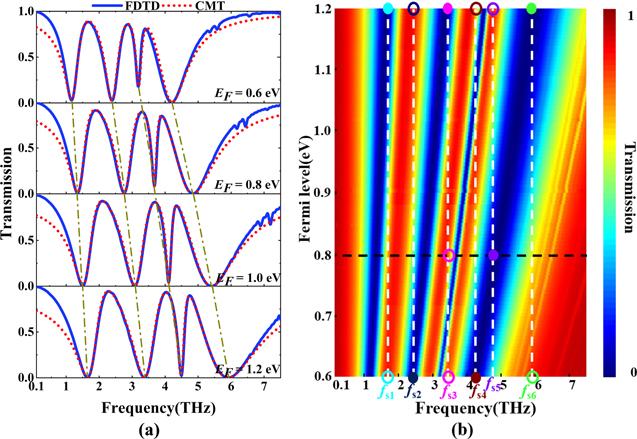
Figure 4. (a) Trasmission spectra obtained by FDTD simulation and CMT calculation at different Fermi levels. (b) The evolution of transmission spectra versus Fermi level and frequency. |
Besides, it can be seen that the four resonant frequencies corresponding to the four dips increase as the increasing of the Fermi levels in figure 4(a). In order to better observe the transmission evolution under continuous changing of the Fermi levels, we draw a three-dimensional planar diagram of the evolution as shown in figure 4(b). It is easy to observe from this figure that the obvious blue shift of the transmission spectra has taken place as the Fermi levels increase. It should be pointed out that when the blue shift occurs with the increasing of the Fermi levels, some resonant dips turn into the transparent windows at different Fermi levels, which provides a theoretical basis for the realization of the optical switch. On this basis, we found that when EF is set to 1.2 and 0.6 eV (or 0.8 eV), the proposed structure can realize the multi-switch modulation function at [fs1, fs2, fs3, fs4, fs5, fs6] = [1.648, 2.382, 3.354, 4.187, 4.742, 5.913] THz as shown in figures 4(b) and 5. When EF = 0.6 eV, the proposed graphene metamaterial realizes the ‘on’ state at [fs1, fs3, fs6] = [1.648, 3.354, 5.913] THz and the ‘off’ state at [fs2, fs4] = [2.382, 4.187] THz. When EF = 1.2 eV, ‘on’ and ‘off’ states are completely opposite. The solid and hollow circles in figures 4(b) and 5 represent the ‘off’ and ‘on’ states of the switches, respectively. Therefore, when EF = 0.6 and 1.2 eV, it can realize a penta-frequency asynchronous and a double-frequency or triple-frequency synchronous optical switches. In addition, it realizes ‘on’ state at fs3 = 3.354 THz and ‘off’ state at fs5 = 4.742 THz when EF = 0.8 eV. ‘on’ and ‘off’ states are opposite when EF = 1.2 eV. Taking into account the nature of the switch, the extinction ratio (ER) is used to express the amplitude modulation [45]
$\begin{eqnarray}\mathrm{ER}=10\times {\mathrm{log}}_{10}\displaystyle \frac{{T}_{\max }}{{T}_{\min }},\end{eqnarray}$
where ${T}_{\max }$ and ${T}_{\min }$ are the transmittances of the ‘on’ and ‘off’ states, respectively. In addition, modulation depth (MD) and insertion loss (IL) are also two key factors to judge the performance of the switch, which can be obtained respectively by the following formulas: $\begin{eqnarray}\mathrm{MD}=\displaystyle \frac{\left|{T}_{\max }-{T}_{\min }\right|}{{T}_{\max }}\times 100 \% ,\end{eqnarray}$
$\begin{eqnarray}\mathrm{IL}=-10\times {\mathrm{log}}_{10}({T}_{\max }).\end{eqnarray}$
After calculations, we give table 1 to clearly display the ER, MD and IL of each switch. One can clearly see that the ranges of MD and IL are (97.30 % ≤ MD ≤ 99.97%) and (0.33 dB ≤ IL ≤ 1.04 dB), respectively, which means that the switching effect of the proposed structure is very superior. In order to highlight the excellent performance of the switches, we also list table 2 to compare the performance of graphene optical switches in different structures. It can be concluded that not only big MD, high ER and low IL are the symbols of the optical switch modulators’ excellent performance, but also the multi-frequency characteristic is a good advantage.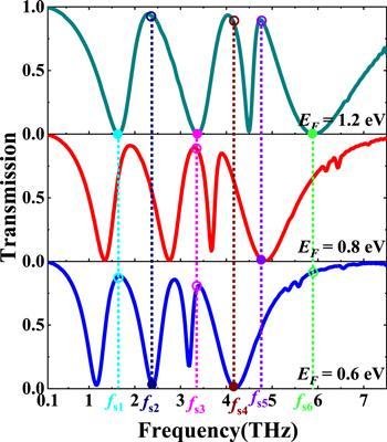
Figure 5. Simulated transmission spectra when EF = 1.2 eV, 0.8 eV and 0.6 eV. |
Table 1. Parameters of the optical switches in the proposed bilayer graphene metamaterial. |
| EF = 1.2 eV | EF = 0.6 (or 0.8) eV | ||||||
|---|---|---|---|---|---|---|---|
| f (THz) | Transmission | on/off | Transmission | on/off | MD (%) | IL (dB) | ER (dB) |
| 1.648 | 0.002 | off | 0.882 | on | 99.76 | 0.55 | 26.20 |
| 2.382 | 0.926 | on | 0.025 | off | 97.30 | 0.33 | 15.68 |
| 3.354 | 0.003 | off | 0.787 | on | 99.58 | 1.04 | 23.80 |
| 0.883 | on | 99.63 | 0.54 | 24.30 | |||
| 4.187 | 0.849 | on | 0.005 | off | 99.39 | 0.71 | 22.18 |
| 4.742 | 0.899 | on | 0.020 | off | 97.82 | 0.46 | 16.61 |
| 5.913 | 0.0003 | off | 0.918 | on | 99.97 | 0.37 | 35.29 |
Table 2. Performance comparison of our metamaterial with other graphene-based structures. |
| Switch effect | Slow light effect | |||||
|---|---|---|---|---|---|---|
| Reference | Modulation | Maximum | Minimum | Modulation | Maximum | Maximum |
| /year | mode | MD | IL | band | τd or ng | DBP |
| [46]/2017 | Single-frequency | 98.90% | 0.83 dB | Terahertz | — | — |
| [47]/2022 | Penta-frequency | 88.10% | 16.80% | Terahertz | 770 | — |
| [48]/2020 | Single-frequency | 83.30% | 7.20% | Terahertz | 150 | — |
| [49]/2022 | Quadruple-frequency | 94.30% | 10.90% | Terahertz | — | — |
| [50]/2020 | Dual-frequency | 93.00% | 0.25 dB | Terahertz | 358 | — |
| [51]/2020 | Penta-frequency | 93.50% | 0.10 dB | Terahertz | 935 | — |
| [52]/2021 | Hepta-frequency | 98.00% | 0.31 dB | Terahertz | 0.488 ps | 0.35 |
| [53]/2021 | — | — | — | Terahertz | 0.250 ps | — |
| [54]/2011 | — | — | — | Near-infrared | ∼26 | 0.31 |
| [55]/2015 | — | — | — | Near-infrared | > 60 | 0.26 |
| Our work | Penta-frequency | 99.97% | 0.33 dB | Terahertz | 0.848 ps | 0.58 |
Generally speaking, PIT effect has great application prospects in optical storage. Because its transparent window shows an extreme dispersion effect, the propagation speed of the electromagnetic wave can be slowed down. The result is that the interaction between light and matter is enhanced, that is, the interaction time between light and matter is increased, which means more light information is stored. Time delay (τd) is an important parameter of the slow-light effect. τd can be expressed as the following equation [56]:
$\begin{eqnarray}{\tau }_{d}=\displaystyle \frac{{\rm{d}}\varphi }{{\rm{d}}\omega },\end{eqnarray}$
where φ = arg(t) is the transmission phase shift. Figures 6(a)–(d) show the curves of time delay and phase shift as a function of the frequency of incident light at different Fermi levels. We successfully understand that the destructive interference of the incident light and the four coupled modes causes serious dispersion in the vicinity of the transparent window, which in turn leads to a sharp change in phase shift and a significant change in time delay. In figure 6(a), the peak values of the time delay are P1 = 0.364 ps, P2 = 0.373 ps and P3 = 0.407 ps. The maximum time delays in figures 6(a)–(d) are 0.407 ps, 0.704 ps, 0.845 ps and 0.848 ps, respectively. We can conclude that the maximum time delay increases as the Fermi level of graphene increases. In other words, as the Fermi level of graphene increases, the slow-light effect is becoming better and better.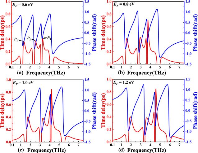
Figure 6. (a)–(d) Evolution of time delay and phase shift with frequency at different Fermi levels of 0.6 eV, 0.8 eV, 1.0 eV and 1.2 eV. |
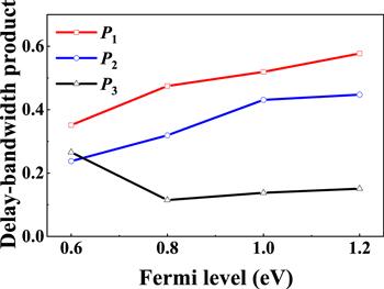
Additionally, the delay-bandwidth product (DBP) is another important parameter to evaluate the slow-light effect, which symbolizes the highest buffering capacity of all slow-light devices. It can be expressed as DBP = τdΔf, where Δf is the 3 dB bandwidth of time delay [57]. The evolution of DBP with EF is shown in figure 7. It can be seen that the smallest DBP is bigger than 0.1. When EF = 1.2 eV, the biggest DBP can reach 0.58, which is higher than 0.31 [54] and 0.26 [55] obtained from other PIT systems, too. In order to highlight the slow-light effect of the proposed structure, we compare our structure with other graphene structures, as shown in table 2. It can be found that our structure has great advantages in slow-light effect compared with most other slow-light devices.
Figure 7. DBP of the time delay peaks versus the Fermi level. |
4. Conclusions
In short, a novel bilayer graphene terahertz metamaterial composed of double graphene ribbons and double graphene rings realizes the dynamically tunable triple-PIT. The simulated transmission spectra by FDTD method fit well with the theoretical results by CMT. It is worth noting that this structure realizes a penta-frequency switching modulator according to the dynamically adjustable triple-PIT effect. The maximum modulation depth (MD) and the minimum insertion loss (IL) of the switch are 99.97% and 0.33 dB, respectively. In addition, the slow-light effect of the proposed structure is also further investigated by the time delay. The results show that when the Fermi level of graphene reaches 1.2 eV, the maximum time delay can reach 0.848 ps, and the biggest DBP is up to 0.58. Consequently, the proposed structure opens up a new idea for the research of multi-frequency optical switches and excellent slow-light devices.