


1. Introduction
With its unique spectral properties, terahertz radiation (usually defined in the frequency range of 0.1 THz to 10 THz) shows prospects in many cutting-edge applications, such as molecular identification, high-resolution imaging, and homeland security [1–6]. For instance, W Miao et al reported a THz high performance hot-electron bolometer detector, which utilized a uniform graphene layer as a microbridge to connect two spiral antennas. Its noise equivalent power was about 15 fW/Hz0.5, its dynamic range reached 47 dB in the range of 0.3 K–10 K, and the optical coupling efficiency was about 58% [7]. Caused by the collective oscillation of electrons, surface plasmons (SPs) propagate along the interface between the metal and dielectrics, which can be utilized to manipulate light on the sub-wavelength structure beyond the diffraction limit. The common SPs waveguides include metal wire structures, metal-dielectrics-metal, channel waveguide structures, and hybrid plasmonic structures [8, 9], which offer a compromise between a long propagation length and good confinement [10–13]. By depositing a dielectric stripe on the metal substrate, the dielectric-loaded surface plasmonic (DLSPs) structure is a typical hybrid waveguide and indicates the advantages of strong optical field confinement capability and low dissipation [14–16].
Tunable functional devices are very important to the further practical applications of plasmonic waveguides [17]. Described by pseudo-relativistic Dirac fermions with linear energy dispersion, Dirac semimetals (DSM) manifest the merits of high mobility, strong plasmonic property and good tunable properties [18]. As a typical 2D DSM, the graphene layer exhibits good tunable electronic transport and is widely investigated in the design of DLSPs [19–23]. For instance, based on a hybrid plasmonic structure of micro-disk resonator configuration, A. Karimi et al suggested a novel temporal integrator in the near-IR spectral region by replacing the noble metal with a uniform graphene layer, which showed the integration time window was about 5.55 ps, 11 times longer than previous samples, and the FWHM bandwidth was 53 GHz with a significantly compact footprint of 4 μm×3 μm [19]. Based on elliptical Ag wires deposited on graphene-Al2O3-Ag substrate hybrid structure, Z Li et al proposed a tunable graphene optical modulator, and its modulation depth and insertion loss were 16.7 dB μm−1 and 0.17 dB μm−1, respectively. The 3 dB bandwidth of the modulator was 200 GHz [20]. Consisting of GaAs cylinder-SiO2 cuboid-graphene-SiO2 substrate structure, X. He et al reported a novel graphene-based hybrid plasmonic waveguide in the THz region, indicating that the normalized modal area reached 0.0018 (λ2/4) at 3 THz and the propagation length can reach as long as a few hundred microns [21]. J. Gosciniak et al presented a graphene-based electro-optic plasmonic modulator with a dielectric ridge, the modulation bandwidth of the suggested structure was more than 15 THz, and waveguide loss was about 0.08 dB [22]. Based on a dielectric cylinder levitated Si-graphene-SiO2 substrate or Si-graphene-Si substrate, S. Qu et al proposed a tunable graphene-based hybrid plasmonic modulator, showing that the modulation depth reached 0.6 dB μm−1 and the insertion loss was 0.05 dB μm−1 [23].
Nowadays, high performance flexible functional devices are in high demand to meet the rapid development of THz technology. Though there is some research work about the graphene DLSPs waveguides, it is still a challenge to modulate the THz hybrid plasmonic mode properties conveniently, due to the restrictions of the graphene thin layer. Similar to graphene, 3D DSM which is also called bulk Dirac semimetal, also manifests high mobility and very good tunability [24–30]. Furthermore, 3D DSMs are easier to process and are more stable compared with 2D graphene membranes. The carrier mobility of 3D DSM (up to 9 × 106 cm2 V−1 s−1 at 5 K) is also much higher than that of graphene at the same temperature (2 × 105 cm2 V−1 s−1) [31–36]. To achieve the manipulation of propagation properties efficiently in the THz regime, we investigate the 3D DSM-supported DLSPs structure, including the effects of Fermi level, the shape of dielectric semielliptical fiber, and operation frequencies. The results manifest that the modulation depth of the normalized effective mode area reaches more than 63%, and the figure of merit (FoM) is more than 220 at a Fermi level of 0.15 eV.
2. Research methods
Figure 1 shows the sketch of the proposed 3D DSM DLSPs waveguide structures. The semielliptical dielectric fiber is deposited on the 3D DSM layer. As given in figure 1(a), ax and by are the semi-minor and semi-major axes of the dielectric semi-ellipse. Figure 1(b) shows the modified 3D DSM-supported SiO2-Si hybrid structures and the semi-elliptical dielectric materials deposited on the 3D DSM layer. In figure 1(b), ax1 and by1 are the semi-minor axis and the semi-major of interior dielectric semi-ellipse, respectively, ax2 and by2 are the semi-minor axis and the semi-major of the exterior dielectric semi-ellipse, respectively.
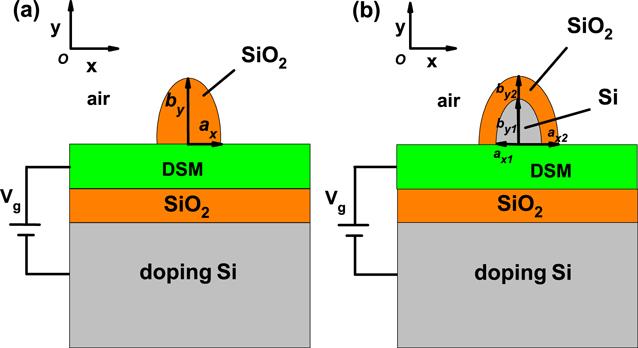
Figure 1. The sketch of the proposed 3D DSM DLSPs waveguide structures. (a) is the sketch of the proposed 3D DSM-supported DLSPs waveguide. The semi-minor axis and the semi-major axis of dielectric semielliptical are ax and by, respectively. (b) is the sketch of the 3D DSM-supported modified DLSPs waveguide. The semi-minor axis and the semi-major axis of the interior dielectric semi-ellipse are ax1 and by1. The semi-minor axis and the semi-major axis of the exterior dielectric semi-ellipse are ax2 and by2. |
The complex conductivity of 3D DSM is given by [25, 26]:
$\begin{eqnarray}\mathrm{Re}\sigma \left({\rm{\Omega }}\right)=\displaystyle \frac{{e}^{2}}{\hslash }\displaystyle \frac{g{k}_{F}}{24\pi }{\rm{\Omega }}G({\rm{\Omega }}/2),\end{eqnarray}$
$\begin{eqnarray}\text{Im}\sigma ({\rm{\Omega }})=\displaystyle \frac{{e}^{2}}{\hslash }\displaystyle \frac{g{k}_{F}}{24{\pi }^{2}}\left\{\begin{array}{l}\displaystyle \frac{4}{{\rm{\Omega }}}\left[1+\displaystyle \frac{{\pi }^{2}}{3}\left(\displaystyle \frac{T}{{E}_{F}}\right)\right]\\ +8{\rm{\Omega }}\displaystyle {\int }_{0}^{{\varepsilon }_{{\rm{c}}}}\left[\displaystyle \frac{G\left(\varepsilon \right)-G\left({\rm{\Omega }}/2\right)}{{{\rm{\Omega }}}^{2}-4{\varepsilon }^{2}}\right]\varepsilon {\rm{d}}\varepsilon \end{array}\right\},\end{eqnarray}$
in which G(E) = n(-E)-n(E), the n(E) is the Fermi distribution function, EF is the Fermi level, kF = EF/ℏvF is the Fermi momentum, vF ≈c/300 is the Fermi velocity, ϵ = E/EF, Ω = ℏω/EF + iℏτ−1/EF, τ = μEF/ev2F = 4.5 × 10⁻¹³ s, and μ is carrier mobility. ϵc = Ec/EF = 3 (Ec is the cutoff energy beyond which the Dirac spectrum is no longer linear), and g = 40 is the degeneracy factor.The mode area is defined as the ratio of the total mode energy and peak energy density [11],
$\begin{eqnarray}{{\rm{A}}}_{{\rm{m}}}=\displaystyle \frac{{W}_{{\rm{m}}}}{\max \left\{W\left(r\right)\right\}}=\displaystyle \frac{1}{\max \left\{W\left(r\right)\right\}}\displaystyle {\int }_{-\infty }^{+\infty }W(r){{\rm{d}}}^{2}r,\end{eqnarray}$
W(r) can be calculated by the following formula: $\begin{eqnarray}W(r)=\displaystyle \frac{1}{2}\left(\displaystyle \frac{{\rm{d}}\left(\varepsilon \left(r\right)\omega \right)}{{\rm{d}}\omega }{\left|E\left(r\right)\right|}^{2}+{\mu }_{0}{\left|H\left(r\right)\right|}^{2}\right),\end{eqnarray}$
in which E(r) and H(r) are the electric and magnetic fields, respectively.The effective index neff can be defined by the following formula:
$\begin{eqnarray}{n}_{{\rm{e}}{\rm{f}}{\rm{f}}}=\beta /{k}_{0},\end{eqnarray}$
in which β is the complex propagation constant, and k0 is the free space wave vector.The propagation length L can be defined by the following formula:
$\begin{eqnarray}L=\lambda /4\pi \text{Im}\left({n}_{{\rm{eff}}}\right).\end{eqnarray}$
The modulation depth (MD) can be given by the following formula:
$\begin{eqnarray}{\rm{MD}}=\left({x}_{{\rm{\max }}}-{x}_{{\rm{\min }}}\right)/{x}_{{\rm{\max }}},\end{eqnarray}$
in which x stands for neff and L.The figure of merits (FoM) of the propagation mode is defined as:
$\begin{eqnarray}{\rm{FoM}}=L/\sqrt{{A}_{{\rm{m}}}}.\end{eqnarray}$
3. Results and discussions
The numerical results have been obtained using the finite element method (FEM) software package-COMSOL MULTIPHYSICS 4.2. The propagation properties of the suggested 3D DSM DLSPs waveguides are shown in figure 2. To have a fair comparison, the cross-sectional areas of semielliptical dielectric fibers are taken as 1 × 104 μm2. The influences of ax on the Re(neff) and propagation lengths of hybrid modes can be found in figures 2(a) and (b), respectively. As the frequency increases, the 3D DSM permittivity decreases, and the contribution of plasmonic mode decreases, resulting in the value of the Re(neff) increasing, and the propagation length decreasing. For example, at the frequencies of 0.5 THz, 1.0 THz, and 2.0 THz, the 3D DSM permittivity are −1.850 × 10⁴ + 1.310 × 10⁴i, −6.162 × 10³ + 2.186 × 10³i and −1.672 × 10³ + 299.5i, respectively. Correspondingly, the values of Re(neff) of hybrid modes are 1.157, 1.720 and 1.914, and the propagation lengths are 1.665 × 104 μm, 9.443 × 103 μm, and 8.417 × 103 μm, respectively. In addition, the semielliptical fiber shape also affects the propagation property significantly. It can be found in figure 2(a), that if the value of the semi-minor axis of dielectric semielliptical fiber is small, i.e. ax < 80 μm, the length of semielliptical fiber along the y direction, by, is large, the mode can be better confined. As the value of ax (by) increases (decreases), some modes leak into the surrounding air, and the real part of the effective index decreases. For example, at the frequency of 1.0 THz, if the value of ax is 60, 100 and 120 μm, the values of the Re(neff) are 1.708, 1.720 and 1.686, and the propagation lengths are 1.423 × 104 μm, 9.443 × 103 μm, and 8.070 × 103 μm, respectively. The mode confinement can be well measured by the normalized effective mode area Am/A0, in which A0 is the diffraction-limited area, and the value is λ2/4. As the frequency increases, the wavelength decreases, and the contribution of fiber mode increases, thus the 3D DSM-supported DLSPs show weak mode confinement at a large frequency, as given in figure 2(c). As the frequency increases, the permittivity of the 3D DSM layer decreases, the influence of the plasmonic mode reduces, and the contribution of dielectric fiber mode increases, resulting in the mode area increasing. To judge the comprehensive performance of mode confinement and dissipation of the hybrid modes, the definition of FoM is given by equation (9 ). As the frequency increases, the contribution of the low lossy fiber mode increases, while the effects of high dissipation plasmonic mode decrease, resulting in the value of FoM increasing. It is clear that the FoM is also closely associated with the fiber shape. As shown in figure 2(d), as the value of ax decreases, the semielliptical fiber becomes sharper, and the interaction area of fiber with the 3D DSM layer reduces, thus the 3D DSM structure manifests better mode confinement and a larger value of FoM.
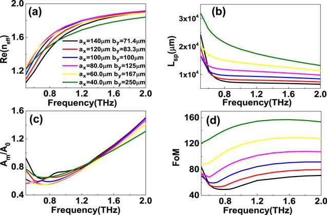
Figure 2. The propagation properties of the 3D DSM-supported DLSPs waveguides versus frequency for different kinds of semielliptical dielectric fiber. (a) is the real part of the effective index. (b) is the propagation length. (c) is the normalized effective mode area. (d) is the figure of merit. The cross-sectional area is set as 1 × 104 μm2. The values of ax are 40, 60, 80, 100, 120, and 140 μm, respectively. The Fermi level of the 3D DSM layer is set as 0.08 eV. |
To learn the propagation properties of 3D DSM modes well, the electric field distribution for different kinds of wave structures is given in figure 3. The frequency is set as 1 THz and the Fermi level is 0.10 eV. As given in figure 3, if the value of the semi-minor axis of dielectric semielliptical fiber is very small, e.g. ax = 40 μm, the semielliptical dielectric fiber cannot provide good mode confinement along the x direction. As the ax increases, the hybrid mode is well confined, which can be found in figures 3(b) and (c). This means that if the semi-elliptical dielectric fiber is relatively sharp, the hybrid mode indicates good mode confinement and low lossy simultaneously, which results from the relatively smaller interaction area of the dielectric fiber and the 3D DSM layer. However, if the semi-minor axis of dielectric semielliptical is very large, a large amount of mode penetrates into the surrounding air, as shown in figures 3(e) and (f). Furthermore, thanks to the larger interaction area of semielliptical fiber with the 3D DSM layer, the dissipation of the hybrid mode is also large simultaneously. For instance, at the operation frequency of 1 THz, the propagation length of 3(b) and 3(f) are 1.423 × 104 μm and 7.084 × 103 μm, respectively. From the above discussion, the suggested 3D DSM semielliptical DLSPs structures show good properties on the condition that the value of ax is relatively small and the value of by is relatively larger, in the next work, the value of ax and by are set as ax = 60 μm, by = 167 μm.
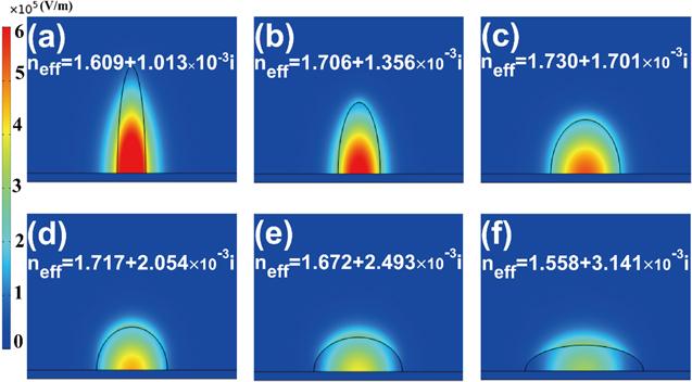
Figure 3. The electric field distributions of the proposed 3D DSM-supported DLSPs waveguides for different kinds of semielliptical dielectric fibers. The frequency is set as 1 THz. The Fermi level of the 3D DSM layer is set as 0.10 eV. The ax are set as 40 μm (a), 60 μm (b), 80 μm (c), 100 μm (d), 125 μm (e), 167 μm (f). Meanwhile, the by are set as 250 μm(a), 167 μm (b), 125 μm (c), 100 μm (d), 80 μm (e), 60 μm (f), respectively. |
Different from the conventional metal substrate, the permittivity of the 3D DSM layer can be changed significantly by changing the Fermi level, which affects the hybrid mode obviously, as shown in figure 4. The dielectric semielliptical material is set as SiO2. In figures 4(a) and (b), as the frequency increases, the permittivity of the 3D DSM layer decreases, the contribution of plasmonic mode decreases, and more modes penetrate into the 3D DSM layer, resulting in the value of the Re(neff) increasing, and the propagation length reducing. For example, at the frequencies of 0.5 THz, 1.0 THz and 2.0 THz, the values of the Re(neff) are 1.259, 1.714 and 1.902, respectively. Additionally, as given in figure 4, the 3D DSM Fermi levels affect the propagation property of the hybrid mode obviously. As the Fermi level increases, the carrier concentration increases drastically, the 3D DSM layer indicates better metal and plasmonic properties. Thus, the skin depth reduces, the propagation length increases, and the FoM also improves significantly. For example, at the frequency is 1.0 THz, if the Fermi levels are set as 0.05 eV, 0.10 eV and 0.15 eV, the 3D DSM permittivity are −2.400 × 10³ + 8.564 × 10²i, −9.634 × 10³ + 3.415 × 10³i and −2.169 × 10⁴ + 7.679 × 10³i, respectively. Meanwhile, the values of the propagation length are 9.073 × 103 μm, 1.760 × 104 μm and 2.715 × 104 μm, and the figure of merit are 76.4, 145, and 223, respectively.
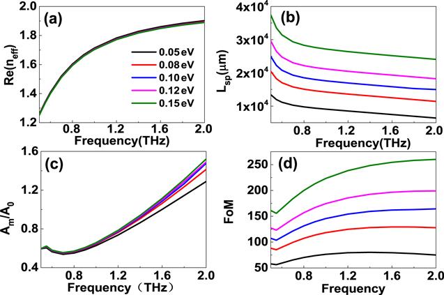
Figure 4. The propagation properties of the 3D DSM-supported DLSPs waveguides versus frequency for different Fermi levels. (a) is the real part of the effective index. (b) is the propagation length. (c) is the normalized effective mode area. (d) is the figure of merit versus frequency for different Fermi levels. The ax is set as 60 μm, the by is set as 167 μm. The Fermi levels are set as 0.05 eV, 0.08 eV, 0.10 eV, 0.12 eV and 0.15 eV, respectively. The material of the dielectric semielliptical is set as SiO2. |
The propagation properties of the hybrid modes are closely associated with the composed materials of dielectric fiber. Figure 5 illustrates the effects of different kinds of dielectric fiber shape on the performance of hybrid modes. As the permittivity of fiber increases, the mode confinement and loss increase, resulting in a smaller propagation length. For instance, for the Si and SiO2 dielectric fiber, at the frequency of 1.0 THz, the real parts of effective indices are 3.204 and 1.706, the propagation lengths are 8.927 × 103 μm and 1.760 × 104 μm, the normalized effective mode areas are 0.382 and 0.649, and the values of the FoM are 96.19 and 145.6 for Si and SiO2, respectively. To have a better understanding of the hybrid plasmonic properties, the composed dielectric semi-ellipses are adopted, i.e. the Si fiber is coated with a thin dielectric layer with a smaller refractive index like SiO2, which can be found in the insets of figure 5(b). Here, it is observed that as the percentages of Si decrease, the real part of the neff decreases, the contribution of dielectric fiber decreases, and the plasmonic mode from the 3D DSM layer enhances, resulting in the mode area decreasing, as given in figure 5(c). Simultaneously, due to the low refractive index of SiO2 increases, the dissipation decreases, the propagation length increases, and the value of FoM increases as well, which can be found in figures 5(b) and (d), respectively. For instance, at the operation frequency of 1 THz, if the structure mode of Si fiber along the x direction is Si0.3ax (18 μm), Si0.5ax (30 μm), Si0.8ax (48 μm), the values of the normalized mode area are 0.3828, 0.1972 and 0.1990, and the values of the FoM are 84.62, 79.45 and 73.95, respectively. The modulation depth of normalized mode area and FoM are 48.48% and 12.61%, respectively.
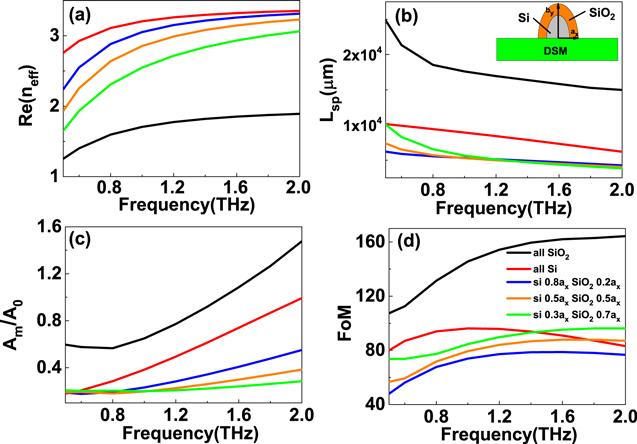
Figure 5. The propagation properties of the 3D DSM-supported DLSPs waveguides versus frequency for different kinds of SiO2-Si hybrid dielectric fiber. (a) is the real part of the effective index. (b) is the propagation length. (c) is the normalized effective mode area. (d) is the figure of merits of different Si semi-ellipse layer structures versus frequency. The value of ax and by is 60 μm and 167 μm, respectively. The height of Si fiber is fixed as 83.3 μm. The Fermi level of the 3D DSM layer is set as 0.10 eV. |
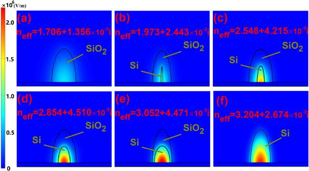
Figure 6 is the field distribution of the 3D DSM-modified DLSPs waveguides. As the refractive index of dielectric fiber increases, the hybrid mode can be better confined near the dielectric fiber and 3D DSM layer, and the loss increases as well, as given in figures 6(a) and (f). For example, the effective indices of hybrid modes are 1.706 + 1.356 × 10⁻³i and 3.204 + 2.674 × 10⁻³i for the SiO2 and Si dielectric fiber. Next, we discuss the Si-SiO2 hybrid dielectric fiber structures. With the increase of Si percentage, the interaction area of Si fiber with the 3D DSM layer increases, resulting in the increasing loss, which can be found in figures 6(b) and (c). But if the Si portion increases further, the lossy dielectric fiber contributes more to the hybrid mode, and the loss reduces. For example, if the lengths of Si fiber along the x direction are Si0.1ax (6μm), Si0.3ax (18μm), Si0.5ax (30μm), Si0.8ax (48μm) the effective indexes of hybrid modes are 1.973 + 2.443 × 10⁻³i, 2.548 + 4.215 × 10⁻³i, 2.854 + 4.510 × 10⁻³i and 3.052 + 4.471 × 10⁻³i, respectively. Additionally, as given in figures 6(b)–(f), the hybrid SiO2-Si dielectric fiber structure indicates better mode confinement, which results from that the semielliptical dielectric SiO2 preventing the hybrid mode from penetrating into the surrounding environment. From the above simulation results, it can be concluded that if the length of Si fiber along x direction is Si0.3ax (18 μm), the hybrid dielectric fiber structure indicates the best performance, the FoM reaches 96.18, and the normalized effective mode area is about 0.2077. Compared with the best performance of a single dielectric fiber structure, the real part of the effective index increases by 61%, and the normalized effective mode area decreases by 65%.
Figure 6. The electric field distribution of the 3D DSM-supported modified hybrid waveguides structure. The frequency is set as 1 THz. The Fermi level is 0.10 eV. The dielectric material of (a) and (f) is SiO2 and Si, respectively. The exterior and interior of (b)–(e) are SiO2 and Si, respectively. The height of Si is 0.5 by. the width of Si is set as 0.1 ax,0.3 ax,0.5 ax and 0.8 ax, respectively. (ax = 60 μm, by = 167 μm). |
4. Conclusion
The tunable propagation properties of the 3D DSM-supported DLSPs waveguide structures have been given and discussed in the THz regime, including the effects of dielectric fiber shape, 3D DSM Fermi level, and operation frequencies. The results manifest that the dielectric semielliptical fiber shape affects the hybrid mode significantly. On the condition that the value of the semi-minor axis of dielectric semielliptical is small, the sharp fiber manifests good mode confinement and low loss simultaneously, and the FoM of hybrid mode reaches more than 220. With the help of 3D DSM, the propagation length can be modulated in the range of 9.073 × 103 μm–2.715 × 104 μm if the Fermi level of the 3D DSM changes in the range of 0.05 eV–0.15 eV, and the corresponding modulation depth is about 65.1%. Additionally, the performance of the hybrid mode can be improved by utilizing the SiO2-Si hybrid dielectric strip, and the value of Re(neff) of the SiO2-Si semielliptical fibers reaches about 3.05 on the condition that the operation frequency is 1 THz, much larger than that of single SiO2 fiber, 1.71; the normalized effective mode area decreases by 65% comparing to single SiO2 fiber. The results are very helpful to understand the propagation mechanism of the hybrid plasmonic structure and to design novel tunable devices in the future, such as switchers, modulators, and sensors.