


1. Introduction
Graphene has gradually become the most concerned two-dimensional material with the honeycomb lattice structure on account of its excellent electronic, mechanical, thermal and optical properties such as ultra-wide optical response spectrum, ultra-fast response time and high carrier mobility [1–3]. As a result, graphene is becoming a versatile material in many applications including sensors [4], perfect absorbers [5], optical switches [6, 7], etc. Further investigations have revealed that graphene can exhibit metalloid properties in a specific frequency region, suggesting that graphene can propagate the transverse magnetic (TM) mode of surface plasmon polaritons (SPPs). Compared to metals, graphene has many superior properties such as its strong field confinement, excellent electrical tunability and low Ohmic losses [8]. The most significant preponderance is that the spectral characteristics of graphene structures can be dynamically modulated by changing the Fermi levels of graphene without changing the structure parameters. Meanwhile, the Fermi levels can be regulated by adjusting the gate voltage. In a word, graphene plasmons are ideal alternatives to noble-metal plasmons in the terahertz band [9, 10]. Because of these foundations and properties, multifunctional devices of devices based on graphene plasmons have been designed and studied.
Plasmon-induced transparency (PIT), a plasmonic analogy of classical electromagnetically induced transparency [11], is a transparent result produced by destructive interference between bright mode and dark mode [12]. The bright mode can be excited directly by incident light with huge radiation loss then generates a transmission valley with low transmittance in the transmission spectrum. Whereas dark mode with small radiation loss can not be excited directly by incident light and exhibits a transmission band with high transmittance in the transmission spectrum. But the dark mode can be excited indirectly by the light field generated by the interaction between the bright mode and the incident light. The resonance of bright mode and dark mode at certain frequency points leads to two transmission dips and a transparent window, which reveals the formation mechanism of PIT. In recent years, PIT based on graphene plays an irreplaceable role in micro-nano sensing. In 2018, Tang et al realized a refractive index sensing sensitivity of 0.36 THz RIU−1 on a graphene micro-ribbon array structure for single-PIT sensing application [13]. In 2020, He et al achieved 1.713 45 THz RIU−1 on a two-graphene sheet structure for the homologous single-PIT sensing application [14]. In 2021, Cui et al put forward three graphene strips with different shapes for dual-PIT sensing applications and obtained a sensing sensitivity of 4.19 THz RIU−1 [15]. In 2022, Li et al achieved 3.4269 THz RIU−1 on a graphene ribbon and U-shaped graphene pattern for dual-PIT sensing application [16]. Although many graphene-based PIT sensors are reported, there are few reports about triple-PIT sensing applications with high sensitivity based on graphene structure.
In this paper, we propose an ultra-high sensitive terahertz sensor based on tunable triple-PIT in a planar monolayer graphene metasurface composed of six graphene blocks and two graphene strips. The simulated results obtained by the finite-difference time-domain (FDTD) method [17, 18] exhibit a dynamically tunable triple-PIT effect when the Fermi levels of graphene increase and the evolution of triple-PIT can be perfectly demonstrated by the coupled mode theory (CMT) [19] analysis. Then, we investigate the sensing performance in the proposed graphene-based structure by altering the surrounding refractive index. The maximum sensitivity and figure of merit (FOM) can reach up to 5.7115 THz RIU−1 and 116.32, respectively. Additionally, the structure exhibits excellent slow-light performance with a maximum group refractive index of up to 1036. Therefore, the proposed structure has tremendous potential for the research of sensors and slow light devices.
2. Structure and theoretical analysis
The three-dimensional schematic diagram of the proposed structure is shown in figure 1(a), which consists of monolayer patterned graphene and the silicon substrate. The graphene metamaterial is periodically distributed in the x–y plane and illuminated by an x-polarized plane wave which is incident perpendicularly along the positive direction of the z-axis. The whole structure is connected by metal electrodes in order to adjust the Fermi levels of graphene by regulating the gate voltage Vg, as shown in figure 1(c). Figure 1(b) shows the top view of one unit cell. It is comprised of four identical big graphene blocks (FBGBs), two same small graphene blocks (TSGBs) and two uniform graphene strips (TGSs). The specific geometric parameters in the figure 1(b) are as follows: Lx = Ly = 6 μm, l1 = 1.6 μm, l2 = 1.4 μm, l3 = 2.4 μm, l4 = 0.4 μm, l5 = 0.8 μm.

Figure 1. (a) Schematic illustration of the proposed graphene metamaterial. (b) Top view of one unit cell. (c) A modulation schematic diagram between the Fermi level of graphene and gate voltage. |
In FDTD simulation, the medium around the structure is air whose relative dielectric constant is 1 and the temperature T is set to 300 K. In figure 1(a), we set the x-axis and y-axis directions as periodic boundary conditions so they can be treated as infinite. The boundary conditions of the z-axis direction are the perfectly matched layers. The conductivity of graphene can be simplified into a Drude-like expression [20]:
$\begin{eqnarray}{\sigma }_{g}=\frac{{\rm{i}}{e}^{2}{E}_{{F}}}{\pi {\hslash }^{2}\left(\omega +{\rm{i}}{\tau }^{-1}\right)},\end{eqnarray}$
where e, EF, ℏ, ω and τ are the electronic charge, the Fermi level of graphene, the reduced Planck constant, the angular frequency of incident light and the carrier relaxation time, respectively. Here, τ = μEF/(eVF2), μ = 1 m2 (V−1 s−1) is the carrier mobility and VF = 106 m s−1 is the Fermi velocity [21]. In addition, the Fermi level EF is modulated by the applied gate voltage according to the following formula [22]: $\begin{eqnarray}{E}_{{F}}=\hslash {V}_{{F}}\sqrt{\frac{\pi {\varepsilon }_{0}{\varepsilon }_{\mathrm{si}}{V}_{g}}{d{e}}},\end{eqnarray}$
where ϵ0 is the vacuum permittivity, ϵsi = 11.9 is the relative permittivity of silicon [23], d is the thickness of the silicon layer and Vg is the gate voltage. Due to the graphene metamaterial is between the substrate silicon and the medium air, the dispersion relation can be solved by Maxwell equations and electromagnetic field boundary conditions, which can be expressed as [24]: $\begin{eqnarray}\displaystyle \frac{{\varepsilon }_{{\rm{si}}}}{\sqrt{{\beta }^{2}-{\varepsilon }_{{\rm{si}}}{{k}_{0}}^{2}}}+\displaystyle \frac{{\varepsilon }_{{\rm{air}}}}{\sqrt{{\beta }^{2}-{\varepsilon }_{{\rm{air}}}{{k}_{0}}^{2}}}=-\displaystyle \frac{{\rm{i}}{\sigma }_{g}}{\omega {\varepsilon }_{0}},\end{eqnarray}$
here, β is the propagation constant, k0 is the wave vector of incident light and ϵair = 1 is the relative permittivity of air.
The designed monolayer patterned graphene structure can achieve a significant triple-PIT phenomenon when it is irradiated vertically from the top along the z-axis by planar light. The transmission spectra of FBGBs, TSGBs and the combined structure of FBGBs and TSGBs are drawn with a green dotted line, purple dotted line and a red dot-dash line respectively in figure 2(a). And the transmission spectra of the combined structure of FBGBs and TSGBs, TGSs and the whole structure are drawn with a red dot-dash line, blue dotted line and a black solid line respectively in figure 2(b). The transmission spectra of FBGBs and TGSs only have one induced transparent window, so they are called single-PIT. In this way, the transmission spectra of the combined structure of FBGBs and TSGBs and the whole structure present the dual-PIT and triple-PIT because they respectively appear as two and three-induced transparent windows. Furthermore, three resonant dips in the transmission spectrum of the combined structure of FBGBs and TSGBs are named dip1′, dip2′, dip3′ from left to right and the corresponding frequencies are f1′ = 6.67 THz, f2′ = 11.66 THz, f3′ = 12.88 THz, respectively. Similarly, four resonant dips in the transmission spectrum of the whole structure are named dip1, dip2, dip3 and dip4. Their corresponding frequencies are f1 = 5.42 THz, f2 = 10.06 THz, f3 = 12.35 THz and f4 = 13.6 THz, respectively.
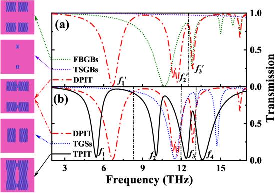
Figure 2. (a) Transmission spectra of FBGBs, TSGBs and the combined structure of FBGBs and TSGBs. (b) Transmission spectra of the combined structure of FBGBs and TSGBs and the whole structure (EF = 1.0 eV). |
In order to further analyze the formation of the PIT effect, we first divide figure 2(a) into two frequency regions with a black vertical dot-dash line. In the first frequency region, there is an obvious transmission dip in the transmission spectrum of the FBGBs structure, so the FBGBs act as a bright mode. In the meantime, the TSGBs act as a dark mode owing to the spectral transmittance in this frequency region is always very high, almost close to 100%. The interaction between the dark mode and the bright mode forms two transmission dips corresponding to dip1′ and dip2′. From the electric field distribution at the frequency of f1′ = 6.67 THz in figure 3(a), we can see that the electric field energy is mainly concentrated on FBGBs and a small amount of it is concentrated on TSGBs. At this time, the bright mode FBGBs is directly excited, and the dark mode TSGBs is indirectly excited by the coupled light field generated by the interaction between the bright mode TSGBs and the incident light. Therefore, the formation of dip1′ is caused by the interaction between the dark mode TSGBs and the bright mode FBGBs. Figure 3(b) shows the distribution of electric field intensity corresponding to dip2′. We can find that the electric field energy is mainly focused on the edges of FBGBs and there is almost no electric field on TSGBs, indicating that the dark mode TSGBs has no effect on the formation of dip2′ and its formation is mainly attributed to the bright mode FBGBs. In the second frequency region, FBGBs act as a bright mode while TSGBs act as a dark mode, too. From figure 3(c) we can find that the electric field energy is mainly concentrated on the edges of FBGBs and there is no electric field energy on TSGBs. So the dark mode is not excited, meaning that the production of dip3′ is mainly relied on the interaction between the bright mode FBGBs and the incident light. The above analysis explains the formation of the dual-PIT generated by the combined structure of FBGBs and TSGBs.

Figure 3. (a)–(c) Distributions of electric field intensity ∣E∣ at the three frequency points f1′, f2′ and f3′. (d)–(g) Distributions of electric field intensity ∣E∣ at the four frequency points f1, f2, f3 and f4. |
Then, we divide figure 2(b) into four frequency regions with three black vertical dot-dash lines to analyse the mechanism of the triple-PIT effect caused by the whole structure. In the first frequency region, the TGSs act as a dark mode while the combined structure of FBGBs and TSGBs acts as a bright mode. The electric field intensity distribution in figure 3(d) shows that most of the electric field energy is concentrated on TGSs and a small part of it is concentrated on the combined structure of FBGBs and TSGBs. Hence, the dark mode is indirectly excited by the light field generated by the interaction between the incident light and the bright mode on the basis that the bright mode is excited directly by the incident light. As a result, the interaction between the TGSs and the combined structure of FBGBs and TSGBs together produces dip1. In the second frequency region, both the TGSs and the combined structure of FBGBs and TSGBs are bright modes. The electric field intensity distribution corresponding to the frequency point f2 is shown in figure 3(e). We can observe that the electric field energy is distributed mainly around the corners of the combined structure of FBGBs and TSGBs and the inside edges of TGSs. Consequently, the two bright modes work together to form dip2. In the third frequency region, the TGSs act as a dark mode and the combined structure of FBGBs and TSGBs acts as a bright mode. From figure 3(f), it can be seen that the electric field energy is mainly distributed at the edges of the combined structure of FBGBs and TSGBs and there is little electric field energy on TGSs. We can conclude that the bright mode is excited by the incident light while the dark mode is not excited, illustrating that the formation of dip3 is attributed to the combined structure of FBGBs and TSGBs. In the last frequency region, the combined structure of FBGBs and TSGBs and the TGSs act as a dark mode and a bright mode, respectively. The electric field energy is mainly distributed around the corners of the combined structure of FBGBs and TSGBs and the vertical edges of TGSs as shown in figure 3(g). So the bright mode is directly excited by the incident light while the dark is indirectly excited, indicating that the interaction between the bright mode and the dark mode forms dip4. Generally, different structures acting as different modes in different frequency regions interact with each other to form the triple-PIT.
Furthermore, CMT [19, 25] is employed to explore the physical mechanism of the triple-PIT phenomenon and fit the transmission spectra which are obtained by FDTD simulations. Figure 4 is the theoretical coupled diagram of CMT, in which A, B, C and D represent four hypothetical resonator modes and their amplitudes are a, b, c and d, respectively. The subscript ‘±' and the superscript ‘in/out' of ${A}_{\pm }^{{\rm{in}}/{\rm{out}}},$ ${B}_{\pm }^{{\rm{in}}/{\rm{out}}},$ ${C}_{\pm }^{{\rm{in}}/{\rm{out}}}$ and ${D}_{\pm }^{{\rm{in}}/{\rm{out}}}$ respectively represent the positive or negative propagating direction of plasmon waves and input or output plasmon waves. μmn (m, n = 1, 2, 3, 4, m ≠ n) represents the mutual coupling coefficient among the four modes. The relationship between the four resonators can be obtained as follows [26]:1 ) and (3 ). Qon is the external loss quality factor of the nth resonant mode. Qin and Qon are satisfied by the following equation, 1/Qtn = 1/Qin + 1/Qon, where, Qtn = fn/Δfn is the total quality factor of the nth resonant mode. fn and Δfn are the resonant frequency and the full width at half maximum of the nth resonant mode, respectively. According to the energy conservation law, the relationships between the hypothetical resonator modes exhibits as follows:
$\begin{eqnarray}\begin{array}{l}\left(\begin{array}{cccc}{\gamma }_{1} & -{\rm{i}}{\mu }_{12} & -{\rm{i}}{\mu }_{13} & -{\rm{i}}{\mu }_{14}\\ -{\rm{i}}{\mu }_{21} & {\gamma }_{2} & -{\rm{i}}{\mu }_{23} & -{\rm{i}}{\mu }_{24}\\ -{\rm{i}}{\mu }_{31} & -{\rm{i}}{\mu }_{32} & {\gamma }_{3} & -{\rm{i}}{\mu }_{34}\\ -{\rm{i}}{\mu }_{41} & -{\rm{i}}{\mu }_{42} & -{\rm{i}}{\mu }_{43} & {\gamma }_{4}\end{array}\right)\cdot \left(\begin{array}{c}a\\ b\\ c\\ d\end{array}\right)\\ =\,\left(\begin{array}{cccc}-{\gamma }_{o1}^{1/2} & 0 & 0 & 0\\ 0 & -{\gamma }_{o2}^{1/2} & 0 & 0\\ 0 & 0 & -{\gamma }_{o3}^{1/2} & 0\\ 0 & 0 & 0 & -{\gamma }_{o4}^{1/2}\end{array}\right)\cdot \left(\begin{array}{c}{A}_{+}^{{\rm{in}}}+{A}_{-}^{{\rm{in}}}\\ {B}_{+}^{{\rm{in}}}+{B}_{-}^{{\rm{in}}}\\ {C}_{+}^{{\rm{in}}}+{C}_{-}^{{\rm{in}}}\\ {D}_{+}^{{\rm{in}}}+{D}_{-}^{{\rm{in}}}\end{array}\right),\end{array}\end{eqnarray}$
γn = iω − iωn − γin − γon, where i, ωn and ω are the imaginary unit, the nth resonant angular frequency and the angular frequency of incident light, respectively. ωn can be calculated by ωn = 2πfn, fn corresponds to f1, f2, f3 and f4 in figure 2(b). γin = ωn/(2Qin) and γon = ωn/(2Qon) represent the decay rate of intrinsic loss and the decay rate of escaping power into outside space in the nth mode, respectively. Qin is the internal loss quality factor of the nth resonant mode, which can be expressed as Qin = Re(neff)/Im(neff) [27]. neff = β/k0 is the effective refractive index. The relationship between β and ω can be obtained from formulas ( $\begin{eqnarray}{D}_{-}^{{\rm{in}}}=0,\end{eqnarray}$
$\begin{eqnarray}{B}_{+}^{{\rm{in}}}={A}_{+}^{{\rm{out}}}\cdot {{\rm{e}}}^{{\rm{i}}{\varphi }_{1}},{A}_{-}^{{\rm{in}}}={B}_{-}^{{\rm{out}}}\cdot {{\rm{e}}}^{{\rm{i}}{\varphi }_{1}},\end{eqnarray}$
$\begin{eqnarray}{C}_{+}^{{\rm{in}}}={B}_{+}^{{\rm{out}}}\cdot {{\rm{e}}}^{{\rm{i}}{\varphi }_{2}},{B}_{-}^{{\rm{in}}}={C}_{-}^{{\rm{out}}}\cdot {{\rm{e}}}^{{\rm{i}}{\varphi }_{2}}\end{eqnarray}$
$\begin{eqnarray}{D}_{+}^{{\rm{in}}}={C}_{+}^{{\rm{out}}}\cdot {{\rm{e}}}^{{\rm{i}}{\varphi }_{3}},{C}_{-}^{{\rm{in}}}={D}_{-}^{{\rm{out}}}\cdot {{\rm{e}}}^{{\rm{i}}\varphi 3},\end{eqnarray}$
$\begin{eqnarray}{A}_{+}^{{\rm{out}}}={A}_{+}^{{\rm{in}}}-{\gamma }_{o1}^{1/2}\cdot a,{A}_{-}^{{\rm{out}}}={A}_{-}^{{\rm{in}}}-{\gamma }_{o1}^{1/2}\cdot a,\end{eqnarray}$
$\begin{eqnarray}{B}_{+}^{{\rm{out}}}={B}_{+}^{{\rm{in}}}-{\gamma }_{o2}^{1/2}\cdot b,{B}_{-}^{{\rm{out}}}={B}_{-}^{{\rm{in}}}-{\gamma }_{o2}^{1/2}\cdot b,\end{eqnarray}$
$\begin{eqnarray}{C}_{+}^{{\rm{out}}}={C}_{+}^{{\rm{in}}}-{\gamma }_{o3}^{1/2}\cdot c,{C}_{-}^{{\rm{out}}}={C}_{-}^{{\rm{in}}}-{\gamma }_{o3}^{1/2}\cdot c,\end{eqnarray}$
$\begin{eqnarray}{D}_{+}^{{\rm{out}}}={D}_{+}^{{\rm{in}}}-{\gamma }_{o4}^{1/2}\cdot d,{D}_{-}^{{\rm{out}}}={D}_{-}^{{\rm{in}}}-{\gamma }_{o4}^{1/2}\cdot d,\end{eqnarray}$
where φ1 = φ2 = φ3 = 0 is the phase difference between resonators A and B, B and C, C and D, since the four resonators are in the same plane.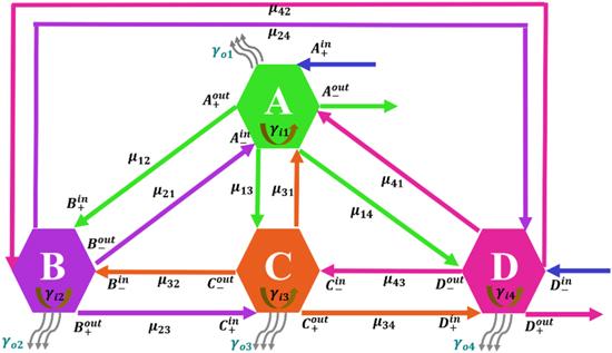
Figure 4. Schematic diagram of CMT. |
With the combination of the above formulas, the transmission coefficient of this system can be obtained by:
$\begin{eqnarray}\begin{array}{l}t=\displaystyle \frac{{D}_{+}^{{\rm{out}}}}{{A}_{+}^{{\rm{in}}}}={{\rm{e}}}^{{\rm{i}}\left({\varphi }_{1}+{\varphi }_{2}+{\varphi }_{3}\right)}-{{\gamma }_{o1}}^{1/2}\cdot {{\rm{e}}}^{{\rm{i}}\left({\varphi }_{1}+{\varphi }_{2}+{\varphi }_{3}\right)}\cdot {D}_{a}\\ \,-\,{{\gamma }_{o2}}^{1/2}\cdot {{\rm{e}}}^{{\rm{i}}\left({\varphi }_{2}+{\varphi }_{3}\right)}\cdot {D}_{b}-{{\gamma }_{o3}}^{1/2}\cdot {{\rm{e}}}^{{\rm{i}}{\varphi }_{3}}\cdot {D}_{c}-{{\gamma }_{o4}}^{1/2}\cdot {D}_{d}.\end{array}\end{eqnarray}$
Here, Da, Db, Dc and Dd can be obtained by: $\begin{eqnarray}\left(\begin{array}{cccc}-{\gamma }_{1} & {\chi }_{12} & {\chi }_{13} & {\chi }_{14}\\ {\chi }_{21} & -{\gamma }_{2} & {\chi }_{23} & {\chi }_{24}\\ {\chi }_{31} & {\chi }_{32} & -{\gamma }_{3} & {\chi }_{34}\\ {\chi }_{41} & {\chi }_{42} & {\chi }_{43} & -{\gamma }_{4}\end{array}\right)\cdot \left(\begin{array}{c}{D}_{a}\\ {D}_{b}\\ {D}_{c}\\ {D}_{d}\end{array}\right)=\left(\begin{array}{c}{{\gamma }_{o1}}^{1/2}\\ {{\gamma }_{o2}}^{1/2}\cdot {{\rm{e}}}^{{\rm{i}}{\varphi }_{1}}\\ {{\gamma }_{o3}}^{1/2}\cdot {{\rm{e}}}^{{\rm{i}}\left({\varphi }_{1}+{\varphi }_{2}\right)}\\ {{\gamma }_{o4}}^{1/2}\cdot {{\rm{e}}}^{{\rm{i}}\left({\varphi }_{1}+{\varphi }_{2}+{\varphi }_{3}\right)}\end{array}\right),\end{eqnarray}$
where $\begin{eqnarray}\begin{array}{lll}{\chi }_{12} & = & {\gamma }_{o1}^{1/2}\cdot {\gamma }_{o2}^{1/2}\cdot {{\rm{e}}}^{{\rm{i}}{\varphi }_{1}}+{\rm{i}}{\mu }_{12},\\ {\chi }_{21} & = & {\gamma }_{o1}^{1/2}\cdot {\gamma }_{o2}^{1/2}\cdot {{\rm{e}}}^{{\rm{i}}{\varphi }_{1}}+{\rm{i}}{\mu }_{21},\end{array}\end{eqnarray}$
$\begin{eqnarray}\begin{array}{lll}{\chi }_{13} & = & {\gamma }_{o1}^{1/2}\cdot {\gamma }_{o3}^{1/2}\cdot {{\rm{e}}}^{{\rm{i}}\left({\varphi }_{1}+{\varphi }_{2}\right)}+{\rm{i}}{\mu }_{13},\\ {\chi }_{31} & = & {\gamma }_{o1}^{1/2}\cdot {\gamma }_{o3}^{1/2}\cdot {{\rm{e}}}^{{\rm{i}}\left({\varphi }_{1}+{\varphi }_{2}\right)}+{\rm{i}}{\mu }_{31},\end{array}\end{eqnarray}$
$\begin{eqnarray}\begin{array}{lll}{\chi }_{14} & = & {\gamma }_{o1}^{1/2}\cdot {\gamma }_{o4}^{1/2}\cdot {{\rm{e}}}^{{\rm{i}}\left({\varphi }_{1}+{\varphi }_{2}+{\varphi }_{3}\right)}+{\rm{i}}{\mu }_{14},\\ {\chi }_{41} & = & {\gamma }_{o1}^{1/2}\cdot {\gamma }_{o4}^{1/2}\cdot {{\rm{e}}}^{{\rm{i}}\left({\varphi }_{1}+{\varphi }_{2}+{\varphi }_{3}\right)}+{\rm{i}}{\mu }_{41},\end{array}\end{eqnarray}$
$\begin{eqnarray}\begin{array}{lll}{\chi }_{23} & = & {\gamma }_{o2}^{1/2}\cdot {\gamma }_{o3}^{1/2}\cdot {{\rm{e}}}^{{\rm{i}}{\varphi }_{2}}+{\rm{i}}{\mu }_{23},\\ {\chi }_{32} & = & {\gamma }_{o2}^{1/2}\cdot {\gamma }_{o3}^{1/2}\cdot {{\rm{e}}}^{{\rm{i}}{\varphi }_{2}}+{\rm{i}}{\mu }_{32}\end{array}\end{eqnarray}$
$\begin{eqnarray}\begin{array}{lll}{\chi }_{24} & = & {\gamma }_{o2}^{1/2}\cdot {\gamma }_{o4}^{1/2}\cdot {{\rm{e}}}^{{\rm{i}}\left({\varphi }_{2}+{\varphi }_{3}\right)}+{\rm{i}}{\mu }_{24},\\ {\chi }_{42} & = & {\gamma }_{o2}^{1/2}\cdot {\gamma }_{o4}^{1/2}\cdot {{\rm{e}}}^{{\rm{i}}\left({\varphi }_{2}+{\varphi }_{3}\right)}+{\rm{i}}{\mu }_{42},\end{array}\end{eqnarray}$
$\begin{eqnarray}\begin{array}{lll}{\chi }_{34} & = & {\gamma }_{o3}^{1/2}\cdot {\gamma }_{o4}^{1/2}\cdot {{\rm{e}}}^{{\rm{i}}{\varphi }_{3}}+{\rm{i}}{\mu }_{34},\\ {\chi }_{43} & = & {\gamma }_{o3}^{1/2}\cdot {\gamma }_{o4}^{1/2}\cdot {{\rm{e}}}^{{\rm{i}}{\varphi }_{3}}+{\rm{i}}{\mu }_{43}.\end{array}\end{eqnarray}$
Therefore, according to the transmission coefficient, we can obtain the transmittance of the proposed triple-PIT system: T = t2.3. Results and discussion
In order to verify the dynamic tunability of the triple-PIT produced by the whole structure, we study the transmission spectra of the proposed graphene metamaterial structure under different Fermi levels, as shown in figure 5(a). In the figure, the blue solid and red dot-dash lines are obtained by FDTD simulation and CMT theoretical calculation, respectively. It can be found that the results fit well, which means that the results of the theoretical calculation are correct. In addition, it can be found that the transmission spectra show a blue shift when the Fermi levels increase. The blue shift phenomenon can also be presented in figures 5(b) and 5(c). It can be seen that frequency points corresponding to three peaks which are named peak 1, peak 2 and peak 3 in the transmission spectra increase with the increasing of Fermi levels. Similarly, the resonant dips (dip1, dip2, dip3 and dip4) also meet this law. This phenomenon can be explained by the resonance condition. The wave vector of surface plasmons along the graphene nanostructure can be expressed by:
$\begin{eqnarray}{k}_{\mathrm{spp}}={\omega }^{2}/\left(2{\alpha }_{0}{E}_{{F}}c\right),\end{eqnarray}$
and it satisfies the relationship kspp ∝ 1/L. Where α0 = e2/(ℏc) and L are the fine nanostructure constants and the length of graphene nanostructure, respectively. Thus, the relationship between graphene plasmon frequency f and the Fermi level EF is as follows: f ∝ (α0EFc/(2π2ℏL))1/2 [28]. From the above formula, we can find that graphene plasmon frequency f is proportional to the square root of the Fermi level EF. The graphene plasmon frequency will become larger with the increase of Fermi level. Thus, the transmission spectra of the proposed graphene metamaterial structure take a blue shift with the increase of the Fermi level.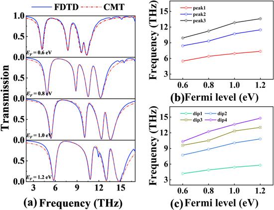
Figure 5. (a) Transmission spectra obtained by FDTD simulation and CMT calculation at different Fermi levels. (b) The resonant frequencies of three peaks versus EF. (c) The resonant frequencies of four dips versus EF. |
Then, we explore the sensing characteristics of the proposed graphene-based structure at different environmental refractive indexes. When the ambient refractive index n increases from 1.0 to 1.1 with a step size of 0.02, the transmission spectra have a red shift and the four dips move to the low frequency direction as shown in figure 6.
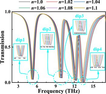
Figure 6. Transmission spectra of the proposed structure at different refractive indexes n = 1.0, 1.02, 1.04, 1.06, 1.08 and 1.1. (EF = 1.0 eV) |
Sensitivity (S) is a critical parameter to measure the sensing performance, which can be expressed as [29]:
$\begin{eqnarray}S=\displaystyle \frac{{\rm{\Delta }}f}{{\rm{\Delta }}n},\end{eqnarray}$
here, Δf is the frequency difference with two adjacent refractive indexes and Δn = 0.02 is the adjacent refractive index difference. We calculate the sensitivities of the four dips at different refractive indexes as shown in table 1. We can obtain the quadruple frequency detection of the sensing performance with the maximum sensitivities of S1 = 3.8075 THz RIU−1 at dip1, S2 = 5.7115 THz RIU−1 at dip2, S3 = 3.81 THz RIU−1 at dip3 and S4 = 5.71 THz RIU−1 at dip4. Additionally, when n changes from 1 to 1.02, S2 can reach up to 5.71 THz RIU−1 at dip2. Similarly, when n changes from 1 to 1.02, 1.04 to 1.06 and 1.08 to 1.1, S4 can also reach up to 5.71 THz RIU−1 at dip4. In a word, by changing the refractive indexes, we can obtain the maximum S of 5.7115 THz RIU−1 at dip2 and several large S with the same value of 5.71 THz RIU−1 at different dips.Table 1. The sensitivities of four dips. |
| Δn | S1 | S2 | S3 | S4 |
|---|---|---|---|---|
| 1.02–1.0 | 1.9035 | 5.71 | 3.81 | 5.71 |
| 1.04–1.02 | 3.8075 | 3.808 | 3.805 | 3.81 |
| 1.06–1.04 | 1.904 | 3.8075 | 3.81 | 5.71 |
| 1.08–1.06 | 3.8075 | 3.8075 | 3.805 | 3.81 |
| 1.1–1.08 | 1.904 | 5.7115 | 3.81 | 5.71 |
Furthermore, a higher FOM is necessary to evaluate the sensing performance with regard to sensors. FOM can be obtained by the following formula [30]:
$\begin{eqnarray}{{\rm{FOM}}}_{\left(f\right)}=\displaystyle \frac{{\rm{\Delta }}T}{T{\rm{\Delta }}n}=\displaystyle \frac{T\left(f,n+{\rm{\Delta }}n\right)-T\left(f,n\right)}{T\left(f,n\right){\rm{\Delta }}n},\end{eqnarray}$
where ΔT is the transmittance difference of the dip, Δn = 0.02, T (f, n + Δn) and T (f, n) are the transmittances at the same frequency f under the refractive indices of n + Δn and n, respectively. According to the transmission spectra at different refractive indexes n and the above formula,we can calculate FOM data when n increases from 1.0 to 1.1 as shown in figures 7(a)–(e). We can observe that the frequency corresponding to the maximum FOM under different n is close to the frequency point of dip4 in the transmission spectra. We can get the maximum FOM of 116.32 at the resonant frequency f = 13.6413 THz as shown in figure 7(a). Based on the above discussion and calculation, our proposed graphene metamaterial structure has ultra-high sensitivity and FOM, and the sensing performance is superior to many other reports. The comparison of sensing performance is listed in table 2.
Figure 7. (a)–(e) Transmission spectra and FOM of the proposed structure at the different refractive indices n = 1.02, 1.04, 1.06, 1.08, and 1.1, respectively. |
Table 2. Performance comparison for the proposed structure with other graphene-based structures. |
| Reference/year | Sensor | Slow light | |
|---|---|---|---|
| Sensitivity | FOM | Group index | |
| [16]/2022 | 3.4269 THz RIU−1 | 21.92 | — |
| [15]/2021 | 4.19 THz RIU−1 | 43.31 | — |
| [14]/2020 | 1.713 45 THz RIU−1 | 6.998 | — |
| [31]/2021 | 1.7745 THz RIU−1 (158 25 nm RIU−1) | 23.61 | — |
| [32]/2022 | 16 660 nm RIU−1 | 31.0924 | — |
| [29]/2022 | 0.7928 THz RIU−1 | 8.12 | 512 |
| [33]/2021 | — | — | 321 |
| [34]/2020 | — | — | 252 |
| [35]/2020 | — | — | 358 |
| [36]/2022 | — | — | 770 |
| Our work | 5.7115 THz RIU−1 (18 350 nm RIU−1) | 116.32 | 1036 |
All in all, the PIT phenomenon has potential applications in optical storage because it shows an extreme dispersion effect near the transparent peak and slows down the propagation speed of the electromagnetic wave. Because of this, the interaction between light and matter will be enhanced and the interaction time will be lengthened, resulting that more light information can be stored. The group refractive index ng depending on the transparency windows of the proposed system is a key parameter to judge the performance of the slow light effect. It can be expressed as follows [37]:13 ). The curves of group index and phase shift are respectively shown in figures 8(b) and 8(a) when the Fermi level is modulated from 0.6 to 1.2 eV with a step size of 0.2 eV. We can see that with the increase of the Fermi level, both the transmission spectra and phase shift will take a blue shift. At a fixed Fermi level, the phase shift oscillates up and down with the increase of frequency, and the oscillation is most obvious at the transmission valleys. In addition, the maximum and minimum phase shifts are up to 1.15 and −1.2 rad respectively when the Fermi level is 1.2 eV. As shown in figure 8(b), the group index also produces a blue shift with the Fermi level increasing. The maximum group index can reach up to 1036 when the Fermi level is 1.0 eV. This value is higher than other slow light effects based on graphene metamaterials with similar parameters, which can be observed in table 2.
$\begin{eqnarray}{n}_{g}=\displaystyle \frac{c}{d}\cdot \displaystyle \frac{{\rm{d}}\phi }{{\rm{d}}\omega },\end{eqnarray}$
where φ = arg(t) is the phase shift of the amplitude transmittance, which can be obtained from the equation (
Figure 8. (a) Evolution of transmission and phase shift with frequency at different Fermi levels of 0.6 eV, 0.8 eV, 1.0 eV and 1.2 eV. (a) Evolution of transmission and group index with frequency at different Fermi levels of 0.6 eV, 0.8 eV, 1.0 eV and 1.2 eV. |
4. Conclusion
Generally speaking, we propose a monolayer patterned graphene metamaterial structure consisting of six graphene blocks and two graphene strips and realize the dynamically tunable triple-PIT effect. The spectral response characteristics of this structure are investigated by numerical simulation and theoretical calculation, and we obtain the fitting curves with a very high matching degree. We have studied the refractive index sensing characteristics of this structure. The obtained maximum sensitivity and FOM are 5.7115 THz RIU−1 (18 350 nm RIU−1) and 116.32, respectively. Significantly, our proposed graphene-based structure can exhibit the quadruple frequency detection of the sensing performance. In addition, we further analyze the slow light effect of the triple-PIT by calculating the group refractive index. The results show that when the Fermi level is 1.0 eV, the maximum group refractive index can reach up to 1036. Hence, the proposed structure provides a new idea for the design of micro-nano sensors and slow light devices.
Acknowledgments
The work is supported by National Natural Science Foundation of China: 61605018, 11904032, 61841503; Science and Technology Project Foundation of the Education Department of Jiangxi Province: GJJ150815.
Declaration of competing interest
The authors declare that they have no known competing financial interests or personal relationships that could have appeared to influence the work reported in this paper.