


1. Introduction
As Moore's law is gradually losing its effectiveness, it is urgent to develop new semiconductor devices with multi-function, low-energy consumption and high-speed operation [1], among which operational agility is crucial for today's microelectronics technology development [2]. Since a semiconductor device often contains a semiconductor nanostructure [3], the transmission time of an electron across a semiconductor nanostructure determines, to some extent, the dynamic response and working speed of the semiconductor devices [4]. Therefore, exploring the transmission time of an electron through semiconductor nanostructures is one of the most important research directions in the field of semiconductor devices [5]. The effective potential functions experienced by an electron in semiconductor devices are, in general, quite complicated, therefore, the transmission time of an electron through semiconductor devices is actually the quantum tunneling time of an electron traversing such effective potentials [6].
Quantum tunneling is one of the most characteristic phenomena in quantum mechanics [7], which is applied extensively in practices, such as quantum tunneling transistors [8]. However, the calculation of transmission time for electron tunneling through a semiconductor device has been an open problem [9]. This tricky issue originates mainly from two aspects: the difficult solution of the Schrödinger equation by the complicated effective potential of electrons in semiconductor devices [10] and the contentious definition and measurement of transmission time in quantum mechanics [11]. Indeed, how long it takes for a particle to tunnel through a potential barrier, which has been confusing physicists for decades, still has no definitive answer to date [12]. An authoritative review [13] lists at least seven different transmission times, including dwell time, group delay (also called phase time), transition time, reflection time, Larmor precession time, Büttiker–Landauer time and complex time. Among these transmission times, dwell time and group delay are, nevertheless, considered well-established in the community [14]. Because of the integral of the module square of the wave function in the potential-barrier region, the calculation of dwell time becomes quite difficult for electrons in semiconductor devices. Fortunately, starting from the Schrödinger equation in quantum mechanics, in 2003 H G Winful (HGW) derived a general relation between the dwell time and the group delay, i.e. the group delay is equal to the dwell time plus a self-interference delay, referred to as the HGW relationship [15]. Thus, the dwell time for an electron through a semiconductor device can be evaluated by subtracting the self-interference delay from the group delay [16], where the group delay and the self-interference delay can be obtained by the energy derivative of the transmission phase shift and the superposition of incident and reflected waves, separately.
Aiming at the complicated problem of calculating the transmission time for an electron to traverse a semiconductor device [17], we propose an alternative numerical approach to evaluate the dwell time of electrons in semiconductor devices, with the help of an improved transfer method (ITMM) [18] and the HGW relationship [15]. Here, we use the ITMM to numerically solve the Schrödinger equation and calculate the dwell time by the HGW relationship for electrons in the semiconductor devices. Compared to the exactly solvable case of rectangular potential-barrier, the established numerical method is demonstrated to be reliable, because it possesses a higher accuracy. Therefore, such a numerical method may be applied to explore the dynamic response and operation speed of the semiconductor device.
2. Theory and numerical method
The electronic tunneling through a semiconductor device considered here is presented in figure 1. In the stationary state description, an electron of energy $E$ and momentum $\hslash {k}_{l}$ is incident from the left upon the semiconductor nanostructure embedded in the semiconductor device that occupies the region ${x}_{-}\lt x\lt {x}_{+},$ where $V(x)$ is the effective potential experienced by an electron in the device and $L={x}_{+}-{x}_{-}$ represents the scale of the device along the electronic transport direction $+x.$ Within the framework of a single particle, effective mass approximation, Schrödinger equation for an electron in the semiconductor device can be written as
$\begin{eqnarray}-\displaystyle \frac{{\hslash }^{2}}{2{m}^{\ast }}\psi ^{\prime\prime} (x)+V(x)\psi (x)=E\psi (x),\end{eqnarray}$
where ${m}^{\ast }=\alpha m$ with a coefficient $\alpha $ stands for the effective mass of an electron in the semiconductor nanostructure, such as ${m}^{\ast }=0.067\,{\rm{m}}$ for GaAs.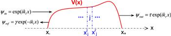
Figure 1. Schematics for electron tunneling through a semiconductor device, where V(x) is the effective potential experienced by an electron in semiconductor nanostructure within the device, as well as x− and x+ represent the region occupied by the device. |
For a practical semiconductor device, the effective potential function $V(x)$ is usually quite complicated, it is therefore impossible to solve equation (1 ) exactly. Here, adopting ITMM [18], we numerically solve the Schrödinger equation of an electron in the semiconductor microelectronics device [19]. In addition, all the physical quantities are used in the dimensionless form for the convenience of discussion and calculation, e.g. $E\to E{E}_{0},$ $x\to x{x}_{0},$ $t\to t{t}_{0},$ etc, where ${x}_{0}=\tfrac{\hslash }{\sqrt{m{E}_{0}}}$ and ${t}_{0}=\tfrac{\hslash }{{E}_{0}}$ are units of length and time, respectively [20]. Without loss of generality, incident, transmitted and reflected waves for an electron can be assumed, separately, by1 ) we divide the device region $[{x}_{-},{x}_{+}]$ into N (≫1) segments, i.e. each segment has the width $d=({x}_{j}^{r}-{x}_{j}^{l})=({x}_{+}-{x}_{-})/N=L/N.$ Due to the very small width in each segment, the potential function can be viewed as a constant such as ${V}_{j}=V({x}_{-}+jd)$ in the jth segment. Thus, the wave function for an electron in the jth segment is expressed by the linear combination of plane waves [21]4a ) and equation (4b ) can be combined into one equation5 ) to each segment from the incident region to the transmitted region, we have
$\begin{eqnarray}\begin{array}{l}{\psi }_{{\rm{in}}}(x)=\exp ({\rm{i}}{k}_{l}x),\,x\lt {x}_{-},\\ {\psi }_{{\rm{out}}}(x)=\tau \exp ({\rm{i}}{k}_{r}x),x\gt {x}_{+},\\ {\psi }_{{\rm{ref}}}(x)=\gamma \exp (-{\rm{i}}{k}_{l}x),x\lt {x}_{-},\end{array}\end{eqnarray}$
in which both wave vectors of an electron in the incident and transmitted regions are ${k}_{l}={k}_{r}=\sqrt{2E};$ while $\tau $ and $\gamma $ represent transmission and reflection amplitudes, respectively. In order to solve equation ( $\begin{eqnarray}{\psi }_{j}(x)={c}_{j}{{\rm{e}}}^{{\rm{i}}{k}_{j}x}+{d}_{j}{{\rm{e}}}^{-{\rm{i}}{k}_{j}x},{x}_{j}^{l}\lt x\lt {x}_{j}^{r},\end{eqnarray}$
where ${k}_{j}=\sqrt{2\alpha (E-{V}_{j})}$ is the wave vector of electron, and ${c}_{j}$ and ${d}_{j}$ are undetermined constants that are determined by the boundary condition of wave functions. According to the continuity of ${\psi }_{j}(x)$ at left and right boundaries of the jth segment (${x}_{j}^{l}$ and ${x}_{j}^{r}$), we have $\begin{eqnarray}{M}_{j-1}^{r}\left(\begin{array}{l}{c}_{j-1}\\ {d}_{j-1}\end{array}\right)={M}_{j}^{l}\left(\begin{array}{l}{c}_{j}\\ {d}_{j}\end{array}\right),\end{eqnarray}$
$\begin{eqnarray}{M}_{j}^{r}\left(\begin{array}{l}{c}_{j}\\ {d}_{j}\end{array}\right)={M}_{j+1}^{l}\left(\begin{array}{l}{c}_{j+1}\\ {d}_{j+1}\end{array}\right),\end{eqnarray}$
where ${M}_{j}^{l}=\left(\begin{array}{l}\exp ({\rm{i}}{k}_{j}{x}_{j}^{l})\,\exp (-{\rm{i}}{k}_{j}{x}_{j}^{l})\\ {\rm{i}}\tfrac{{k}_{j}}{\alpha }\exp ({\rm{i}}{k}_{j}{x}_{j}^{l})\,-{\rm{i}}\tfrac{{k}_{j}}{\alpha }\exp (-{\rm{i}}{k}_{j}{x}_{j}^{l})\end{array}\right)$ and ${M}_{j}^{r}=\left(\begin{array}{l}\exp ({\rm{i}}{k}_{j}{x}_{j}^{r})\,\exp (-{\rm{i}}{k}_{j}{x}_{j}^{r})\\ {\rm{i}}\tfrac{{k}_{j}}{\alpha }\exp ({\rm{i}}{k}_{j}{x}_{j}^{r})\,-{\rm{i}}\tfrac{{k}_{j}}{\alpha }\exp (-{\rm{i}}{k}_{j}{x}_{j}^{r})\end{array}\right)$ may be called the left and right matrixes of the jth segment, separately. Clearly, equation ( $\begin{eqnarray}{M}_{j-1}^{r}\left(\begin{array}{l}{c}_{j-1}\\ {d}_{j-1}\end{array}\right)={M}_{j}{M}_{j+1}^{l}\left(\begin{array}{l}{c}_{j+1}\\ {d}_{j+1}\end{array}\right),\end{eqnarray}$
in which ${M}_{j}=\left(\begin{array}{l}\cos ({k}_{j}d)\,-\tfrac{\sin ({k}_{j}d)}{{k}_{j}/\alpha }\\ ({k}_{j}/\alpha )\sin ({k}_{j}d)\,\cos ({k}_{j}d)\end{array}\right)$ is referred to as the transfer matrix in the jth segment. Applying equation ( $\begin{eqnarray}\begin{array}{l}\left(\begin{array}{l}\exp ({\rm{i}}{k}_{l}{x}_{-})\,\exp (-{\rm{i}}{k}_{l}{x}_{-})\,\\ {\rm{i}}{k}_{l}\exp ({\rm{i}}{k}_{l}{x}_{-})\,-{\rm{i}}{k}_{l}\exp (-{\rm{i}}{k}_{l}{x}_{-})\end{array}\right)\left(\begin{array}{l}1\\ \gamma \end{array}\right)\\ =\,M\left(\begin{array}{l}\exp ({\rm{i}}{k}_{r}{x}_{+})\,0\\ {\rm{i}}{k}_{r}\exp ({\rm{i}}{k}_{r}{x}_{+})\,0\end{array}\right)\left(\begin{array}{l}\tau \\ 0\end{array}\right),\end{array}\end{eqnarray}$
where the total transfer matrix is $M={M}_{1}\times {M}_{2}\,\times \cdots \times {M}_{N}\equiv \left(\begin{array}{l}{m}_{11}\,{m}_{12}\\ {m}_{21}\,{m}_{22}\end{array}\right).$ Thus, transmission and reflection amplitudes can be obtained from the above equation, respectively, by [22] $\begin{eqnarray}\tau =\displaystyle \frac{2{k}_{l}{{\rm{e}}}^{{\rm{i}}({k}_{l}{x}_{-}-{k}_{r}{x}_{+})}}{({k}_{l}{m}_{11}+{k}_{r}{m}_{22})+{\rm{i}}({k}_{l}{k}_{r}{m}_{12}-{m}_{21})},\end{eqnarray}$
$\begin{eqnarray}\gamma ={{\rm{e}}}^{{\rm{i}}2{k}_{l}{x}_{-}}\displaystyle \frac{({k}_{l}{m}_{11}-{k}_{r}{m}_{22})+{\rm{i}}({k}_{l}{k}_{r}{m}_{12}+{m}_{21})}{({k}_{l}{m}_{11}+{k}_{r}{m}_{22})+{\rm{i}}({k}_{l}{k}_{r}{m}_{12}-{m}_{21})}.\end{eqnarray}$
In light of equations (7a ) and (7b ), the group delay and the self-interference delay can be calculated, separately, by [23]
$\begin{eqnarray}{t}_{g}=\displaystyle \frac{{k}_{r}}{{k}_{l}}{\left|\tau \right|}^{2}\displaystyle \frac{\partial [{\rm{Arg}}(\tau )+{k}_{l}({x}_{+}-{x}_{-})]}{\partial E}+{\left|\gamma \right|}^{2}\displaystyle \frac{\partial [{\rm{Arg}}(\gamma )]}{\partial E},\end{eqnarray}$
$\begin{eqnarray}{t}_{i}=-\text{Im}(\gamma )\displaystyle \frac{\partial \,\mathrm{ln}\,{k}_{l}}{\partial E}.\end{eqnarray}$
From the HGW relationship [15], the dwell time of an electron is thus evaluated by $\begin{eqnarray}{t}_{d}={t}_{g}-{t}_{i}.\end{eqnarray}$
3. Reliability of numerical method
To test the above numerical method for calculating the dwell time of an electron through a semiconductor device, we apply it to the exactly solvable situation of a single rectangular potential barrier (SRPB), in which $V(x)={V}_{0},$ a constant in the region between ${x}_{-}=0$ and ${x}_{+}=L.$ For simplicity, we assume ${m}^{\ast }=m,$ i.e. $\alpha =1.$ For the rectangular barrier, the Schrödinger of an electron can be solved analytically, viz, the wave function for an electron in the barrier region reads11a ). However, $k={\rm{i}}k^{\prime} ={\rm{i}}\sqrt{2({V}_{0}-E)}$ for $E\lt {V}_{0},$ where an electron tunnels through the potential barrier and its dwell time is written by11b ). Therefore, the dwell time reads ${t}_{d}={t}_{g}-{t}_{i}$ with the help of the HGW relationship, which is the same as in equations (11a ) and (11b ). In figure 2, we give exactly-calculated dwell time versus the electronic energy (the dotted curve), where the height and width of the rectangular potential barrier are taken as ${V}_{0}=1.0$ (in the unit of ${E}_{0}=1{\rm{meV}}$) and $L=6.66$ (in the unit of ${x}_{0}=\tfrac{\hslash }{\sqrt{m{E}_{0}}}\approx 8.69\,{\rm{nm}}$), respectively, as well as the dwell time is in the unit of ${t}_{0}=\displaystyle \frac{\hslash }{{E}_{0}}\approx 0.66{\rm{fs}}.$
$\begin{eqnarray}\psi (x)=c{{\rm{e}}}^{{\rm{i}}kx}+d{{\rm{e}}}^{-{\rm{i}}kx},\,0\lt x\lt L,\end{eqnarray}$
where $c=\left(1+\tfrac{{k}_{0}}{k}\right){{\rm{e}}}^{-{\rm{i}}kL}/z$, $d=\left(1-\tfrac{{k}_{0}}{k}\right){{\rm{e}}}^{{\rm{i}}kL}/{z}$, $z=2\,\cos \,kL\,-{\rm{i}}\left(\tfrac{{k}_{0}}{k}+\tfrac{k}{{k}_{0}}\right)\sin \,kL\equiv \left|z\right|{{\rm{e}}}^{{\rm{i}}\alpha }$, ${k}_{0}=\sqrt{2E}$, and $k=\sqrt{2(E-{V}_{0})}.$ Therefore, the dwell time for an electron in the rectangular potential barrier is obtained by $\begin{eqnarray}\begin{array}{l}{t}_{d}=\displaystyle \frac{1}{{k}_{0}}\displaystyle {\int }_{{x}_{-}}^{{x}_{+}}{\left|\psi (x)\right|}^{2}{\rm{d}}x=\displaystyle \frac{L{\cos }^{2}\alpha }{2{k}_{0}}\left\{\left[1+{\left(\displaystyle \frac{{k}_{0}}{k}\right)}^{2}\right]{\text{sec}}^{2}(kL)\right.\\ \,\left.\,+\left[1-{\left(\displaystyle \frac{{k}_{0}}{k}\right)}^{2}\right]\displaystyle \frac{\tan (kL)}{kL}\right\},\end{array}\end{eqnarray}$
in which $\alpha =-{\tan }^{-1}\left[\left(\tfrac{{k}_{0}}{k}+\tfrac{k}{{k}_{0}}\right)\tfrac{\tan (kL)}{2}\right].$ Note that the wave vector $k$ of an electron in the barrier region is either real or imaginary. When $E\gt {V}_{0}$ ($k$ is a real number), the dwell time is revealed just as in equation ( $\begin{eqnarray}\begin{array}{l}{t}_{d}=\displaystyle \frac{L{\cos }^{2}\alpha }{2{k}_{0}}\left\{\left[1-{\left(\displaystyle \frac{{k}_{0}}{k^{\prime} }\right)}^{2}\right]\text{sec}{h}^{2}(k^{\prime} L)\right.\\ \left.\,+\,\left[1+{\left(\displaystyle \frac{{k}_{0}}{k^{\prime} }\right)}^{2}\right]\displaystyle \frac{\tanh (k^{\prime} L)}{k^{\prime} L}\right\},\,E\lt {V}_{0},\end{array}\end{eqnarray}$
where $\alpha =-{\tan }^{-1}\left[\left(\tfrac{{k}_{0}}{k^{\prime} }-\tfrac{k^{\prime} }{{k}_{0}}\right)\tfrac{\tanh (k^{\prime} L)}{2}\right].$ In fact, the dwell time for an electron in a rectangular barrier is also obtained by the HGW relationship. It is easy to find transmission and reflection amplitudes as $\begin{eqnarray}\tau =2{{\rm{e}}}^{-{\rm{i}}{k}_{0}L}/z;\,\gamma ={\rm{i}}\left(\displaystyle \frac{k}{{k}_{0}}-\displaystyle \frac{{k}_{0}}{k}\right)\sin \,kL,\end{eqnarray}$
where $z=2\,\cos \,kL-{\rm{i}}\left(\tfrac{k}{{k}_{0}}+\tfrac{{k}_{0}}{k}\right)\sin \,kL\equiv \left|z\right|{{\rm{e}}}^{{\rm{i}}\alpha }$ and $\alpha =-{\tan }^{-1}\left[\left(\tfrac{k}{{k}_{0}},+,\tfrac{{k}_{0}}{k}\right)\tfrac{\tan \,kL}{2}\right].$ Thus, group delay and self-interference delay can be calculated by $\begin{eqnarray}\begin{array}{l}{t}_{g}=-\displaystyle \frac{\partial \alpha }{\partial E}\\ =\,\displaystyle \frac{L{\cos }^{2}\alpha }{2{k}_{0}}\left\{\left[1+{\left(\displaystyle \frac{{k}_{0}}{k}\right)}^{2}\right]{\text{sec}}^{2}kL-{\left(\displaystyle \frac{k}{{k}_{0}}-\displaystyle \frac{{k}_{0}}{k}\right)}^{2}\displaystyle \frac{\tan \,kL}{kL}\right\},\end{array}\end{eqnarray}$
$\begin{eqnarray}{t}_{i}=-\displaystyle \frac{\text{Im}(\gamma )}{{k}_{0}}\displaystyle \frac{\partial {k}_{0}}{\partial E}\,=\displaystyle \frac{L{\cos }^{2}\alpha }{2{k}_{0}}\left[1-{\left(\displaystyle \frac{{k}_{0}}{k}\right)}^{2}\right]\displaystyle \frac{\tan \,kL}{kL}.\end{eqnarray}$
In the above equations, the electron energy is greater than the height of the potential barrier, i.e. $E\gt {V}_{0};$ when $E\lt {V}_{0},$ wave vector $k$ is imaginary and these delays change their forms as in equation (On the other hand, the dwell time of an electron in the rectangular potential barrier can also be evaluated by using the established numerical method in section 2 . To this end, we divide the barrier region into $N=1000$ segments, namely, each segment has the width $d=6.66\times {10}^{-3}.$ The transfer matrix for the jth segment
$\begin{eqnarray}{M}_{j}=\left(\begin{array}{l}\cos \,{k}_{j}d\,-\,\sin \,{k}_{j}d/{k}_{j}\\ {k}_{j}\,\sin \,{k}_{j}d\,\cos \,{k}_{j}d\end{array}\right),\end{eqnarray}$
where ${k}_{j}=\sqrt{2(E-{V}_{0})}$ is the wave vector for an electron in the jth segment. In the numerical calculation, all relevant physical quantities are expressed as double precision data and the program is written and debugged by Fortran language. The dwell time for an electron in the rectangular potential barrier obtained by the numerical method is also presented in figure 2 (dashed curve), where barrier parameters are the same as in the analytical method (dotted curve).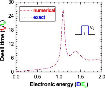
Figure 2. Dwell time for an electron in the SRPB (see the inset) is calculated numerically (dashed curve) and exactly (dotted curve), respectively, where the potential barrier is set to be V0 = 1.0 and L = 6.66, and energy, length and time are in units of 1.0 meV, 8.69 nm and 0.66 fs, respectively. |
Comparing the dashed line to the dotted line in figure 2, both lines overlap very well. This indicates that the dwell time of an electron in the rectangular potential barrier, calculated by different approaches (exact and numerical), is highly consistent. At the same time, it also demonstrates that our developed numerical method possesses very high accuracy, very small calculation error, and very high reliability. Therefore, such a numerical method can be used very well for calculating the dwell time for an electron in a semiconductor microelectronics device.
4. Application of numerical method
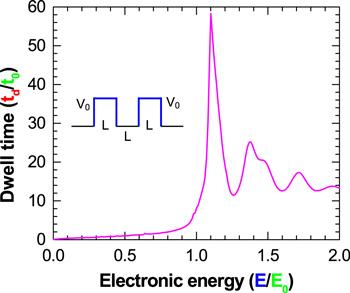
As an application of the developed numerical method in section 2 , we evaluate the dwell time for electrons in double rectangular potential barriers (DRPB) (see the inset of figure 3). In figure 3, we present that the dwell time (${t}_{d}$) changes with the incident energy ($E$) for electron tunneling through the DRPB, where the rectangular potential barrier has the identical height (${V}_{0}=1.0$) and width ($L=6.66$), and the spacing between the two barriers is also L, and the units of physical quantities are the same as in figure 2. Compared with the SRPB, the electrons spend a longer time in the DRPB, approximately twice as much. In general, the dwell time of an electron spent in a potential structure becomes longer, as the number of potential barriers increases. In addition, the spectrum of the dwell time for an electron in the DRPB exhibits a more complicated resonant structure in contrast to the SRPB, which can be understood from the symmetric double potential-barrier structure (where electrons tunnel resonantly through the DRPB).
Figure 3. Dwell time varies with incident energy for an electron in the DRPB, where the height and width of both potential barriers are set to be V0 = 1.0 and L = 6.66 (their spacing is also L), respectively, and the units for energy, length and time are the same as in figure 2. |
5. Conclusions
In summary, we have established a numerical method for calculating the dwell time of electrons in semiconductor devices. In this approach, the dwell time is chosen as the transmission time and the ITMM approach is employed to numerically solve the Schrödinger equation for an electron in the semiconductor device. Compared to the exactly solvable situation of the rectangular potential barrier, the established numerical method has high accuracy and small error, which can fully meet the needs of exploring dynamic response and operation speed of semiconductor devices.
Acknowledgments
This work was supported jointly by the National Natural Science Foundation of China (11864009 and 62164005) and by the Guangxi Natural Science Foundation of China (2021JJB110053).
Declaration of interest
The authors declare that they have no known competing financial interests or personal relationships that could have appeared to influence the work reported in this paper.