


1. Introduction
The terahertz wave range is 3000–30 μm [1–3]. Its electromagnetic wave is consistent with the infrared light in the shortwave band and the millimeter wave in the longwave band [4, 5]. It covers macro theory, micro quantum, and other disciplines [6, 7]. Since the terahertz band includes characteristic spectra of semiconductors, plasma, biology, and biological macromolecules, terahertz has high application value in the fields of material science, military science and technology, information and communication technology, confidential communication, and medical technology [8–11]. The terahertz band is very important in astrophysics because terahertz radiation contains most of the luminosity of the Universe and 98% of the photons generated by the Big Bang are in the THz frequency domain.
Tunable metamaterials are an important component of various optical devices but these materials are extremely rare in the terahertz frequency range [12–16]. After Tao et al designed the first THz absorber based on metamaterials in 2008 [17], metamaterial-based absorbers have attracted extensive research and attention [18–22]. In 2014, Wang et al designed a bandwidth absorber in the THz band through alloy metamaterials. The absorber has two perfect absorption peaks, which can reach an absorption rate of more than 0.9 in the range of about 3 THz and can be tuned by the physical parameters of the absorber [23]. In 2015, Wen et al designed a bandwidth absorber using gold and the absorption rate of the absorber was higher than 0.9 in the 4.4 THz–5.2 THz [24]. In 2016, Guo et al designed an infrared band absorber using metal. Its absorption rate in the 7.9 THz–12 THz is higher than 0.9, and the characteristics of the absorber can be tuned through physical parameters [25]. As a tunable metamaterial with good response in the terahertz range, graphene has been extensively studied as an absorbent [26–30]. It can dynamically adjust Ef by applying a bias voltage to change its electrical characteristics [31–34]. In 2016, Wang et al used multilayer graphene to design a bandwidth absorber that can be in the range of 3–3.8 Thz and can tune the characteristics of the absorber through physical parameters and Ef [15]. In 2018, Yang et al used a dielectric material and graphene to design a bandwidth absorber with an absorption rate higher than 0.9 in the 1.6 THz–3.1 THz [16]. In 2018, Liu et al designed a tunable THz absorber using single-layer graphene, and its absorption at 7–9.25 THz was higher than 0.9 [35]. It can be seen that the THz bandwidth absorber based on single-layer graphene still has great research value.
In this paper, an active tunable terahertz bandwidth absorber based on single-layer graphene is proposed. When the Ef is 1.5 eV, the absorber consists of a layer of graphene and a layer of optical crystal plate, and the substrate is gold. The absorber continuously absorbs electromagnetic waves with high absorption (higher than 0.9) rate in the range of 4.3 THz. The overall absorption rate of the absorber is 96.8% at 3.7–8 THz and there are perfect absorption peaks at 4.1 THz and 6.7 THz. By setting two different modes (TE and TM), the absorber shows good polarization incoherence. The change of relative impedance Z in the absorption frequency band is analyzed. Then, by observing the electric field of 4.1 THz and 6.7 THz, the relationship between the absorption mechanism of the absorber and the geometric parameters is analyzed. The absorber can also tune the absorption characteristics of the absorber by changing the Ef of graphene. Especially, when the Ef of graphene is 2, the high absorption region of the absorber was up to 4.6 THz. Also, fine absorption stability can be maintained under different electromagnetic wave incidence angles. The excellent characteristics of the absorber mean that it has high application value in many fields.
2. Structure design and unit cell model
In this paper, the proposed absorber unit cell consists of three layers, with graphene on the top layer and gold on the substrate separated by a layer of photonic crystal slab (PCS). Figure 1 shows the top view (figure 1(a)) and a structural drawing of the absorber (figure 1(b)). Through simulation analysis and the optimization of CST Microwave Studio, the proposed efficient broadband absorber is simulated and the periodic boundary conditions are applied to the simulation of infinite periodic elements [36–38]. Through careful optimization, the parameters of the absorber are obtained. The P is 60 μm. l1, l2, l3 and l4 are 10 μm, 3.16 μm, 5 μm and 45 μm respectively. The top of the absorber is graphene and its thickness is 1 nm, the PCS below is 11 μm, and the gold is 300 nm.
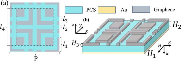
Figure 1. (a) The plane of the absorber and (b) a structural drawing of the absorber. |
The conductivity of graphene can be derived from the famous Kubo formula, and its final result is as follows [39]:
$\begin{eqnarray}\sigma \left(\omega \right)=\displaystyle \frac{{{\rm{e}}}^{2}{E}_{f}}{\pi {\hslash }^{2}}\displaystyle \frac{{\rm{i}}}{\omega +{\rm{i}}{\tau }^{-1}},\end{eqnarray}$
where the $\tau =\mu {E}_{f}/{\rm{e}}{{v}_{f}}^{2}$ is carrier relaxation lifetime and the carrier density μ is $10,000\,{{\rm{cm}}}^{2}\,{{\rm{V}}}^{-1}{{\rm{s}}}^{-1}.$The Fermi velocity is ${v}_{f}=c/300$ and the dielectric constant of graphene can be confirmed by [40]:
$\begin{eqnarray}\varepsilon =1+\displaystyle \frac{{\rm{i}}\sigma \left(\omega \right)}{{\varepsilon }_{0}t\omega },\end{eqnarray}$
where t is the thickness of the graphene, and ϵ0 is the permittivity of the vacuum. The dielectric constant of the PCS is 1.56.3. Results and discussion
S11 is obtained through CST simulation calculation. Then the absorption rate is defined as A = 1–${\left|{S}_{11}\right|}^{2}.$ Figure 2(a) is the absorption spectrum of the different polarization electromagnetic wave incidence. It is obvious that the absorber has strong absorption (greater than 0.9) at 3.7–8 THz and the total absorption rate is 96.8%. The absorption spectra show perfect absorption peaks at λ1 = 4.1 THz and λ2 = 6.7 THz. From the absorption spectra in both polarization modes (the polarization direction of TE is the x-axis and the polarization direction of TM is the y-axis), it is obvious that the absorber exhibits excellent polarization incoherence. Due to the symmetry of the structure, when the electromagnetic waves with different polarization modes are absorbed, the electric dipole will produce similar vibration, which is shown as polarization incoherence on the macro level. Generally speaking, the absorber shows high absorption characteristics when the relative impedance of the absorber is the same as the impedance in the space. The relative impedance Z of the absorber can be determined by [41, 42]:
$\begin{eqnarray}Z=\pm \sqrt{\displaystyle \frac{1+{{S}_{11}}^{2}-{S}_{21}^{2}}{1-{{S}_{11}}^{2}-{S}_{21}^{2}}}.\end{eqnarray}$
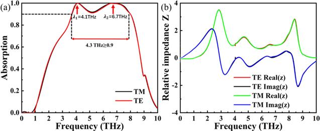
Figure 2. (a) Absorption spectra in two polarization modes (TM and TE) (b) Relative impedance under two polarization modes (TM and TE). |
Figure 2(b) shows the relative impedance of the absorber under the two polarization modes. It is obvious that when the absorber shows high absorption (3.7 THz–8 THz), the relative impedance of the absorber is drawn near space impedance, and when the absorption of the absorber is not high, the relative impedance is far away from the space impedance. At the same time, the relative impedance of the two modes is almost the same, which more intuitively reflects the polarization incoherence of the absorber.
Figure 3 shows the electric field diagram and a locally enlarged diagram of the absorber under the two modes. For the convenience of discussion, the absorber is divided into four areas and the local magnified view of the absorber comes from these areas. For the convenience of discussion, the absorber is divided into four zones, zones 1, 2, 3 and 4 (figure 3(a)). The local magnified view of the absorber comes from these areas. Figure 3(b) shows that when the TE wave is at λ1 = 4.1 THz, the absorber mainly passes through the strong electric field coupling effect of zones 2, 3 and 4, which is due to the electric dipole resonance caused by the horizontal electric field [43–45]. The resonance coupling mainly depends on the properties, shape and scale of the material. This response of the absorber means that the structure proposed in this paper is reasonable and effective. According to figure 3(c), we can see that when the TE wave is λ2 = 6.7 THz, the absorber has the strong electric field coupling effect of zones 1, 2 and 3, and the strong vibration generated by the electric dipole makes the electromagnetic wave lose a lot of energy, thus showing a very high electromagnetic wave absorption rate.
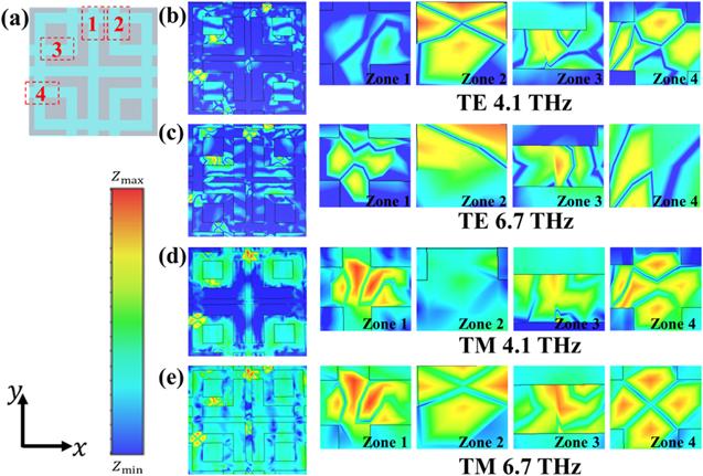
Figure 3. (a) Absorber area division diagram (b) Electric field of TE wave at 4.1 THz (c) Electric field of TE wave at 6.7 THz (d) Electric field of TM wave at 4.1 THz (e) Electric field of TM wave at 6.7 THz. |
Figure 3(d) shows that when the TM wave is λ1 = 4.1 THz, the absorber mainly passes through the strong electric field coupling effect of Zone 1, Zone 3 and Zone 4. Similarly, according to figure 3(e), when the TM wave is λ2 = 6.7 THz, the absorber mainly passes through the strong electric field coupling effect of Zone 1, 2, 3 and 4. According to the vibration position of each Zone, we can infer that the absorption characteristics of the absorber may be related to the geometric parameters. This means that the absorption characteristics of the absorber can be changed by adjusting the geometric parameters.
In order to demonstrate the conjecture, we observe the change in the absorption spectrum of the absorber by changing different physical parameters. In figure 4(a), by changing the performance of the P-tuned absorber, we can see that when P rises from 44 μm to 76 μm, the absorption spectrum undergoes a redshift. The perfect absorption peak is around 4.6 THz when the P is 44 μm. The perfect absorption peak is around 4.4 THz when the P is 52 μm. The perfect absorption peak is around 3.9 THz and 6.3 THz when the P is 68 μm. As the absorber performance declines, there are absorption peaks around 3.8 and 6.8 THz when the P is 76 μm.
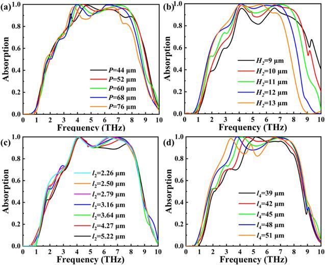
Figure 4. Influence of geometrical parameters on absorber characteristics. (a) Absorber characteristics change with P, (b) absorber characteristics change with H2, (c) and absorber characteristics change with l2. (d) Absorber characteristics change with l4. |
From figure 4(b), it is obvious that the absorption spectrum of the absorber shows a red shift as H2 increases from 9 μm to 13 μm. When ${H}_{2}$ is 9 μm, the absorption efficiency of the absorber is not significant, and the absorption peaks appear at 4 THz and 6.5 THz. When ${H}_{2}$ is 10 μm, the absorption peak of the absorber also appears at 4 THz and 6.5 THz, and the absorption efficiency is further improved. When ${H}_{2}$ is 12 μm, the perfect absorption peak is at 4 THz and 6.8 THz. The high absorption position of the absorption spectrum at this time is higher than that at H2 = 11, but the absorption range at this time is only 3.9 THz (3.5–7.4 THz). When H2 is 13 μm, the perfect absorption peak is at 4 THz and 5.5 THz, and the strong absorption range is only 3.5 THz (3.5 THz–7 THz). It can be seen that with the increase of H2, the strong absorption of the absorption spectrum will be enhanced but the strong absorption range will be reduced, so the appropriate H2 can be selected according to the needs.
Figure 4(c) shows the absorption spectra of the absorber at different l2. It is obvious that the absorption spectra show a slight blue shift with the increase of l2. The variation range of l2 in the figure is 2.26 μm–5.22 μm. It can be found that the absorption peak near 4.1 THz will not be affected by the variation of l2, but with the gradual increase of l2, the perfect absorption peak near 6.7 THz gradually weakens and has a significant blue shift, which ultimately leads to the absorption rate of the absorber for electromagnetic waves near 6.7 THz dropping to around 0.9. As can be seen from figure 3, when l2 is changed, the affected location is mainly zone 1. By comparing figures 4(b) and (c), it can be inferred the reason for this phenomenon is that the absorber absorbs TE waves at 6.7 THz, part of which comes from the strong electromagnetic coupling effect in Zone 1, while changing l2 has an impact on the strong electromagnetic coupling effect there, thus causing the absorber to reduce its absorption of TE wave at 6.7 THz.
Figure 4(d) shows the absorption spectra at different the l4. It is obvious from the figure that as the l4 increases from 39 μm to 51 μm, the absorption spectra will have a redshift. When the l4 is 39 μm, there are absorption peaks near 5.2 THz and 7 THz in the absorption spectrum, where 5.2 THz is the perfect absorption peak and the high absorption part is about 3 THz (4.5–7.5 THz). When the l4 is 42 μm, the absorption spectrum has a perfect absorption peak near 4.6 THz and 6.7 THz and the high absorption part is about 3.7 THz (3.9–7.6 THz). When the l4 is 48 μm, the absorption spectrum has perfect absorption peaks around 3.8 THz and 6.7 THz. Meanwhile, the high absorption part of the absorber is 3.6 THZ–8 THz, but the absorption rate of about 1 THz is lower than 0.9 (4.5–5.5 THz). When the l4 is 51 μm, the absorption spectrum has a perfect absorption peak near 3.4 THz and 6.7 THz. Meanwhile, the high absorption part of the absorber has 3.5 THz (3–3.8 THz, 4.5–4.8 THz, and 5.7–8.1 THz). It is obvious that with the increase of the l4, the absorption peak near 6.7 THz basically remains unchanged, while the redshift of the other absorption peak is more obvious. It is obvious from figure 3(a) that when l4 is changed, zone 1 and zone 4 will be affected. By comparing figure 3(a) and figure 3(b), it can be inferred that this phenomenon is due to the absorption of 4.1 THz partly due to the strong electric field coupling effect in zone 4 [46]. Changing the l4 will affect it, thus the absorption peak changed. It can be considered that in the above results, we change the strength and position of the dipole resonance in some zones by changing the physical parameters so that the whole absorber shows different characteristics.
In general, by changing the physical parameters of the absorber such as the absorption position and absorption width, other indicators of the absorber can be effectively tuned, which indicates that the absorber has a strong physical tuning ability.
Due to the excellent Ef tuning property of graphene, this paper has deeply studied the influence of graphene Ef change on the absorption spectrum, as shown in figure 5. It is obvious that when Ef is increased from 1 eV to 2 eV, the absorption spectrum is blueshifted and the position of the absorption peak changes (figure 5(a)). Figure 5(b) is a partially enlarged view of figure 5(a). It is obvious that when Ef is 1 meV, the absorption peaks of the absorber appear at 3.7 THz and 5.8 THz. At this time, only the absorption of 1.4 THz is higher than 0.9 (3.5–3.8 THz). When Ef is 1.25 eV, the absorption peak of the absorber appears at 3.8 THz and 6.2 THz. At this time, the absorption of about 3.8 THz of the absorber is greater than 0.9 (3.6–7.4 THz). When Ef is 1.75 eV, the absorption peak of the absorber appears at 4.3 THz and 7.5 THz. At this time, the absorber has about 4.6 THz absorption greater than 0.9 (3.8–8.4 THz). When Ef is 2 eV, the absorption peak of the absorber appears at 4.3 THz and 7.5 THz. At this time, the absorber has about 4.6 THz absorption greater than 0.9 (4–8.6 THz). In conclusion, by changing Ef, absorption peaks λ1 and λ2 will move to different degrees, and the high absorption range and the intensity of the absorption peak of the absorber will change accordingly [47]. The shift range of absorption peak λ1 is 3.7–4.3 THz, and the shift range of absorption peak λ2 is 5.8–7.5 THz.
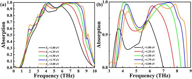
Figure 5. (a) Absorber characteristics Ef.(b) Partially enlarged view of (a). |
The high absorption range span of the absorber is between 0.9–4.6 THz. In the case mainly discussed in this paper (Ef = 1.5 eV), the absorption peaks λ1 and λ2 are perfect (higher than 0.99). The strong absorption range of the absorber is 4.3 THz (3.7–8 THz). It is obvious that the absorber has excellent tunability. Table 1 shows the comparison of the characteristics between different graphene broadband absorbers and the absorber proposed in this paper.
Table 1. Different graphene broadband absorbers. |
| Absorber | Material | Absorption bandwidth | Tuning method |
|---|---|---|---|
| The absorber | Monolayer graphene | 4.3 THz (3.7 THz–8 THz) | Ef and Physical parameters |
| Absorber 1[15] | Multilayer graphene | 0.8 THz (3 THz–3.8 THz) | Ef and Physical parameters |
| Absorber 2 [16] | Dielectric materials and graphene | 1.5 THz (1.6 THz–3.1 THz) | Untuned |
| Absorber 3 [23] | Alloy | 3 THz (1.7 THz–4.7 THz) | Physical parameters |
| Absorber 4 [24] | Gold | 0.8 THz (4.4 THz–5.2 THz) | Physical parameters |
| Absorber 5 [25] | Alloy | 4.1 THz (7.9 THz–12 THz) | Physical parameters |
| Absorber 6 [35] | Monolayer graphene | 2.5 THz (7 THz–9.5 THz) | Ef and Physical parameters |
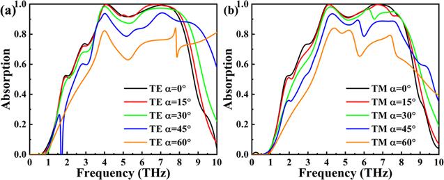
In order to enhance the practicability of the absorber, the influence of different electromagnetic wave incidence angles(α) on the absorber is investigated here, and the results are shown in figure 6. It is obvious that when the α increases from 0° to 30°, the absorbers show good stability (most of them maintain the absorptivity above 0.9 in 3.7–8THz). However, the absorption rate of the absorber mostly drops below 0.9 when the α is 45°. When the α is 60°, the absorptivity will be lower than 0.8. Due to the good polarization-independent property of the absorber, the absorption spectra of both mode waves at different α are basically the same.
Figure 6. Absorption spectrum at different incident angles. (a) TE wave (b) TM wave. |
4. Conclusion
This paper proposes a graphene-based terahertz bandwidth absorber. The absorber shows high absorption at 3.7–8 THz, and there are perfect absorption peaks at 4.1 THz and 6.7 THz. The absorber shows good polarization independence, and the relative impedance in the absorption region is approximate to that in free space. Through the analysis of the electric field diagram, the strong electric field coupling effect that brings about strong absorption is discussed, and by exploring the influence of physical parameters on the absorber, it is found that the absorber shows very high physical adjustability. Subsequently, the Ef was adjusted, and it was found that the absorber had good tunability. This means that the absorber will show excellent tunability by tuning the physical parameters and Ef. Finally, by studying the influence of different incident angles on the absorption spectrum, it is found that the absorber has a certain stability under different α. In general, the absorber can be used in medical research. Military science and technology, space exploration, and other fields have huge application prospects and have a certain role in promoting the research of THz band bandwidth absorbers.