


Introduction
Vibration spectroscopy is a superior biosensing technology that can accurately identify and detect molecules [1]. It mainly relies on the specific vibrations that occur in molecules in the mid-infrared range (37.5–100 THz) [2–4] and can identify molecules and molecular structure/orientation based on the absorption of polar molecular bonds at specific frequencies [5]. In this technology, the absorption film acting as an antenna can guide light to biomolecules (lipids, proteins, polymers, etc) at a specific absorption frequency, thereby enhancing the inherent absorption signal of molecular bonds [6–11].
Electromagnetic absorption films [12, 13] have many vital applications in the infrared (IR) range, such as selective IR thermal emitters, radiation cooling and IR stealth [14–18]. For example, by high absorption/emission of electromagnetic waves within the frequency band of the IR atmospheric transmission window (ATW; 23–37.5 THz and 60–100 THz), energy absorption by the atmosphere can be avoided, thereby keeping the temperature of the object below the ambient temperature. In IR stealth, a high absorption/emissivity in the atmospheric absorption window (AAW; 37.5–60 THz) is required [15].
Previous studies have highlighted the challenges in designing intelligent absorption films with a simple structure that can be tuned by multiple factors and switch between ultra-wideband and narrowband responses [19, 20]. However, recent advances in materials such as Dirac semimetals and vanadium dioxide (VO2) have made the realization of intelligent absorption films possible. Dirac semimetals have attracted considerable interest due to their unique optical properties [21–25]. These materials exhibit an excellent photoelectric response in the high-frequency band and can be tuned through methods such as doping and biasing [21–23]. As a result, they are often referred to as three-dimensional graphene and find extensive applications in the design of optical devices [26–32]. VO2, on the other hand, is an important phase change material that can undergo a lattice structure transformation under temperature control, leading to a macroscopic change from a dielectric state to a metallic state [33–36]. The phase transition of VO2 is reversible, allowing for the design of temperature-controlled optical devices [35–42]. Notably, VO2 has been utilized in the development of tunable devices such as smart windows [43, 44]. Based on the aforementioned characteristics, it is feasible to design an absorption film utilizing Dirac semimetals and VO2. By employing voltage/doping and temperature control, the electromagnetic properties of the film can be tuned, enabling different electromagnetic couplings and the selection of specific absorption bands. This approach enables the creation of a versatile intelligent absorption film.
This paper presents a novel intelligent absorption film that demonstrates dual-tunable ultra-wideband/narrowband switching capabilities. The film achieves multi-band absorption within the frequency range of 30–45 THz or it can achieve absorption with a bandwidth of 94 THz (with an absorption rate exceeding 0.9) within the 30–130 THz range by controlling the temperature. The relative impedance of the absorption film aligns with the impedance matching theory, and its symmetrical structure results in strong polarization incoherence. The film can be tuned through various means, including doping/voltage, temperature and structural parameter adjustments. Furthermore, by adjusting the structural parameters, the absorption film can achieve diverse multi-band absorption responses within the sensing band, indicating its strong tunability. Additionally, when the background refractive index is modified, we observed that most modes within the sensing band exhibit high sensitivity to refractive index changes. This characteristic renders the absorption film highly promising for applications in fields such as biomedicine, where excellent sensing performance is crucial. Moreover, the absorption film exhibits a wider bandwidth and higher absorption rate in the bandwidth absorption response while also demonstrating a certain level of insensitivity to incident angles. These properties make the absorption film a viable candidate for applications in fields such as biosensing and IR stealth.
Structure design and unit cell model
Figure 1(a) shows the structure of the absorption film proposed in this paper. The top layer is a ring of AlCuFe quasicrystals. The lower layer of the ring consists of a layer of VO2 film and a photonic crystal slab (PCS) layer. The bottom layer is a gold substrate. The thickness of the gold substrate is 0.3 μm, which is much greater than the skin depth of electromagnetic waves in the operating frequency range of the absorbing film, preventing the propagation of electromagnetic waves under the film. The ring's outer radius is R1 and the inner radius is R2; the other parameters are indicated in the figure. The absorption film has a period P, which is equal in the x and y directions. The absorption film in this paper is simulated by CST Microwave Studio, launched by CST Company.
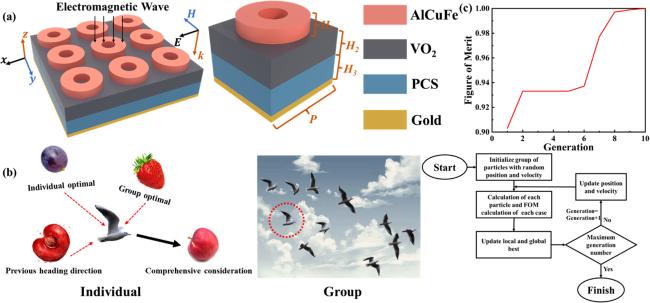
Figure 1. (a) Structure diagram of absorption film. (b) Particle swarm optimization (PSO) algorithm. (c) PSO process. |
A particle swarm optimization (PSO) algorithm was introduced to optimize the structure of the model in order to obtain the optimal physical parameters. The PSO algorithm is a stochastic optimization technique based on population behavior that emulates the collective behavior of bird swarms to search for the optimal solution. Each individual within the swarm adjusts its exploration strategy through personal learning and the shared experiences of other members [44, 45]. Figure 1(b) shows the principle and method of implementation of the PSO algorithm.
We have chosen an improved PSO algorithm to optimize the search steps and reduce the number of iterations. The iterative formulae for updating the velocity and position are as follows:
$\begin{eqnarray}\begin{array}{c}newv=wv+{c}_{1}\ast rand\ast \left(gbest-x\right)\\ +\,{c}_{2}\ast rand\ast \left(pbest-x\right),\end{array}\end{eqnarray}$
$\begin{eqnarray}newx=x+newv,\end{eqnarray}$
$\begin{eqnarray}w={w}_{\max }-\displaystyle \frac{d}{\max \,d}\ast {w}_{\min },\end{eqnarray}$
where $w$ is the inertia weight, $v$ and x are the current velocity and position, ${newv}$ and ${newx}$ are the updated velocity and position, ${c}_{1}$ and ${c}_{2}$ are acceleration constants, ${rand}$ is a random number between 0 and 1 and ${gbest}$ and ${pbest}$ are global and local optimal parameters, respectively.The PSO algorithm provides parameters for model optimization and then updates the optimal parameter values based on the calculation results of the parameter set. When the judgment conditions are met, the parameter set is optimal. The PSO algorithm in the paper will be judged based on the figure of merit (FOM) at T = 353 K, which is defined as
$\begin{eqnarray}FOM=\displaystyle \frac{{f}_{H}}{{f}_{0}},\end{eqnarray}$
where fH is bandwidth with an absorption rate higher than 0.9 in the 35 THz and 130 THz frequency bands and f0 is 95 THz. As shown in figure 1(c), when the parameters are updated to the 10th generation, the absorption rate of the absorption film in the 35–130 THz band is greater than 0.9, and the optimal parameters are set to P = 5.2 μm, H1 = 1 μm, H2 = 2.4 μm, H3 = 2.66 μm, R1 = 2 μm and R2 = 0.86 μm.The Kubo formula in the random phase approximation theory can be used to determine the conductivity of AlCuFe quasicrystals as Dirac semimetals [24, 27]
$\begin{eqnarray}\mathrm{Re}\left(\sigma \left({\rm{\Omega }}\right)\right)=\displaystyle \frac{{{\rm{e}}}^{2}}{\hslash }\displaystyle \frac{g{k}_{F}}{24\pi }{\rm{\Omega }}\theta \left({\rm{\Omega }}-2\right),\end{eqnarray}$
$\begin{eqnarray}\text{Im}\left(\sigma \left({\rm{\Omega }}\right)\right)=\displaystyle \frac{{{\rm{e}}}^{2}}{\hslash }\displaystyle \frac{g{k}_{F}}{24\pi }\left\{\displaystyle \frac{4}{{\rm{\Omega }}}-{\rm{\Omega }}\,\mathrm{ln}\left(\displaystyle \frac{4{E}_{{\rm{c}}}^{2}}{\left|{{\rm{\Omega }}}^{2}-4\right|}\right)\right\},\end{eqnarray}$
where Fermi momentum kF is defined as Ef/ℏvF, Ef is the Fermi level, the Fermi velocity vF is c/300, ${\rm{\Omega }}=\hslash \omega /{E}_{f}+i\hslash {\tau }^{-1}/{E}_{f},$ $\mu $ is carrier mobility, $\hslash {\tau }^{-1}={\nu }_{F}/({k}_{F}\mu )$ and ${\varepsilon }_{c}={E}_{c}/{E}_{f}$, where ${E}_{c}$ is the cut-off energy. The degeneracy factor g of AlCuFe is equal to 40. On this basis, the dielectric constant of AlFeCu quasicrystals can be described as follows [25, 27, 29]: $\begin{eqnarray}\varepsilon ={\varepsilon }_{b}+\displaystyle \frac{{\rm{i}}\sigma }{\omega {\varepsilon }_{0}},\end{eqnarray}$
where ${\varepsilon }_{b}=1$ and ${\varepsilon }_{0}=1$ is the dielectric constant of the background environment.The Drude formula is often used to describe the composite dielectric constant of VO2 [37]
$\begin{eqnarray}\varepsilon \left(\omega \right)=-{\varepsilon }_{\infty }\displaystyle \frac{{\omega }_{p}^{2}}{{\omega }^{2}-{\rm{i}}\omega {\rm{\Gamma }}},\end{eqnarray}$
where ${\varepsilon }_{\infty }$ = 12 is dielectric permittivity at the infinite frequency, ${\rm{\Gamma }}$ is represents the carrier collision time. ${\omega }_{p}$ is the conductivity dependent plasma frequency [37] $\begin{eqnarray}{\omega }_{p}^{2}\left(\sigma \right)=\displaystyle \frac{\sigma }{{\sigma }_{0}}{\omega }_{p}^{2}\left({\sigma }_{0}\right),\end{eqnarray}$
${\sigma }_{0}=3\times 1{0}^{5}\ {\rm{S}}\ {{\rm{m}}}^{-1}$,${\omega }_{p}\left({\sigma }_{0}\right)=1.4\times 1{0}^{15}\,\mathrm{rad}\ {{\rm{S}}}^{-1}$ and $\sigma $ is as shown in figure 3(a). In addition, the dielectric constant of the PCS is 1.56.
Results and discussion
The absorption film optimized by the PSO algorithm has a very novel absorption response at T = 313 K, as shown in figure 2(a). There is multi-band absorption in the 30–45 THz band of the absorption film (as shown in figure 2(b)). This band has strong application prospects in sensing fields such as biomedicine. In addition, at 45–130 THz, the absorption film exhibits a bandwidth absorption of about 85 THz with an absorption rate higher than 0.8. In the sensing band, the absorber has seven absorption peaks M1–M7, located at 34.62, 38.55, 40.26, 40.99, 42.3, 43.6 and 44.63 THz, and absorption rates are 0.99, 0.91, 0.92, 0.98, 0.85, 0.99 and 0.74, respectively. In addition, due to the highly symmetrical design of the absorption film, it can also be seen from figure 2(b) that the absorption film exhibits polarization incoherence. According to the impedance matching theory, when the relative impedance of an absorption film approaches the relative impedance of free space Z0 the absorption film exhibits strong electromagnetic wave absorption, and the relative impedance can be determined by equation 10 (Z0 is about 376.7 Ω. It is related to the electric field and magnetic field generated by electromagnetic waves in free space. When the relative impedance is approximate to the free space impedance, the real part is close to 1 and the imaginary part is close to 0) [46]
$\begin{eqnarray}Z=\pm \sqrt{\displaystyle \frac{{\left(1+{S}_{11}\right)}^{2}-{S}_{21}^{2}}{{\left(1-{S}_{11}\right)}^{2}-{S}_{21}^{2}}}.\end{eqnarray}$
Here S11 and S21 are the coefficients related to scattering and transmission, respectively. It is evident from figure 2(c) that near the absorption peak, the relative impedance Z of the absorption film approaches 1 in the real part and 0 in the imaginary part, while in the non-absorption band Z does not match Z0.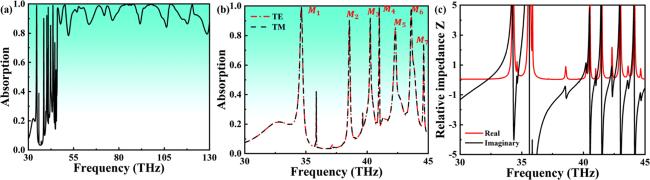
Figure 2. (a) Absorption spectrum of the absorption film. (b) Absorption spectrum in the 30–45 THz range. (c) Relative impedance Z. |
VO2 is an important phase change material and its conductivity can be controlled by temperature. As the temperature increases, the VO2 lattice transforms from a monoclinic insulator to a rutile metal, which gradually weakens the non-metallic properties of VO2 and enhances its metallicity. The phase transition temperature of VO2 is around 340 K, indicating that the change of phase transition of VO2 is gradually apparent at 340 K. When the temperature is below 340 K, VO2 mainly exhibits dielectric properties. When the temperature is higher than the phase transition temperature, the metallic state of VO2 is enhanced, After complete phase transition (at approximately 345 K), VO2 mainly exhibits metallic properties. As shown in formula 5, the conductivity of VO2 is closely related to $\sigma $ [47]. The change of $\sigma $ during heating and cooling of VO2 is shown in figure 3(a). In addition, we can see from figure 3 that the 30–45 THz absorption spectrum gradually shifts from seven-band absorption to bandwidth absorption as the temperature increases. Moreover, at 353 K the absorption film has an absorption bandwidth of about 94 THz in the 30–130 THz band with an absorption rate higher than 0.9. Interestingly, when VO2 is completely transformed into a metallic state, we obtained an ultra-wideband of approximately 93 THz in the 30–130 THz frequency range, and the absorption rate was more stable than at 313 K (the absorption rate of the ultra-wideband absorption was always greater than 0.9).
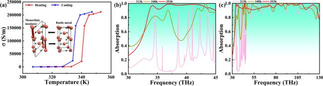
Figure 3 (a) $\sigma $ during heating and cooling. (b) The changes in the absorption spectrum at 30–45 THz. (c) The changes in the absorption spectrum at 30–130 THz. |
Figure 4(a) shows the absorption spectrum of the absorption film at 353 K: the structure of VO2 has completely transformed into a rutile metal, which means that VO2 mainly shows metallic behavior. It can be seen that the bandwidth of the absorption film is about 93 THz (34–127 THz), and the absorption rate will remain above 0.9, which means that the absorption film has broad application prospects in fields such as IR stealth. The absorption film shows the property of polarization incoherence. At the same time, the relative impedance of the absorption film in figure 4(b) also indicates that the absorption film conforms to impedance matching theory. It is worth pointing out that ultra-wideband covers the AAW and ATW bands, giving the absorption film the potential to become an important mid-infrared electromagnetic absorption device.

Figure 4. (a) Absorption spectrum. (b) Relative impedance Z. |
Figure 5 shows the scanning spectrum of the absorption film at 313–353 K (figure 5(a) in the 30–45 THz band and figure 5(b) in the 30–130 THz band). We can see from figure 3(a) that when the temperature reaches around 340 K, the atomic lattice of VO2 will change from monoclinic insulator to rutile metal, and the macroscopic properties of VO2 will gradually transform from a dielectric state to a metallic state. It is evident that in the 30–45 THz band, when the temperature gradually increases from 313 K to 335 K, the absorption film still exhibits a seven-band absorption optical response. Subsequently, as the temperature reaches 340 K, VO2 gradually transforms into a metallic state, and the optical response gradually transforms into bandwidth absorption, reaching a stable state when phase transition is completed (at about 343 K). Figure 5(b) shows that when the temperature is lower than the phase transition temperature, the bandwidth of the absorption wave of the absorption film shows multiple defects with an absorption rate lower than 0.8. As the temperature increases, the absorption band of the absorber film gradually stabilizes. Finally, at a temperature of 353 K, the absorption rates of the absorption band are all greater than 0.9. Figure 5(c) depicts the absorption rate of each mode as well as the average absorption rate within the 35–130 THz band. Notably, modes 1, 2, 3, 4 and 6 exhibit a decrease in absorption rate with increasing temperature. This phenomenon can be attributed to the increased metallicity of VO2, resulting in a weakened localized surface plasmon resonance (LSPR) effect [48, 49]. Conversely, mode 5 displays an increase in absorption rate as the temperature rises. This suggests that as VO2 transitions into a metallic state, the enhancement of guided-mode resonance coupling and electromagnetic coupling leads to higher energy absorption in mode 5. Additionally, mode 7 initially weakens and subsequently strengthens with increasing temperature. This behavior is due to the fact that, at a certain temperature, the gain introduced by guided-mode resonance coupling surpasses the loss caused by the weakening of the LSPR effect [50]. Overall, as the temperature rises, the metallic state of VO2 amplifies the effects of guided-mode resonance and electromagnetic coupling, thereby enhancing the overall electromagnetic absorption capacity [51]. This gain can be more distinctly observed around the phase transition point (approximately 340 K).
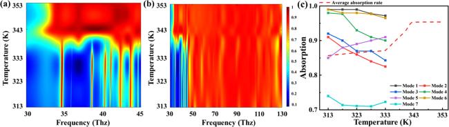
Figure 5. Scanning spectrum of the absorption film at 313–353 K: (a) the 30–45 THz band; (b) the 30–130 THz band. (c) Absorption rate. |
In order to study the corresponding physical mechanism of the absorption of the absorption film, we analyzed the electric field distribution of the absorption film. Figure 6 shows the electric field distribution of the absorption film in different states. It is obvious that in 34.5 THz mode the absorption of the absorption film is mainly excited by the guided-mode resonance coupling of the VO2 layer in the dielectric state. As the temperature increases, VO2 begins to transition to the metallic state, the guided-mode resonance coupling in the VO2 layer disappears and the electric field concentration gradually shifts towards the AlCuFe layer. After VO2 completes the phase transition to the metallic state, the absorption mainly comes from the LSPR effect that occurs at the interface between AlCuFe and VO2 [52]. When the mode is 37 THz at 313 K the absorption film does not exhibit any electromagnetic coupling effect and the absorption response of the absorption film is relatively weak. When the temperature increases, due to the metallization of VO2, the LSPR effect appears at the interface between AlCuFe and VO2, resulting in an absorption response [53]. At 125.4 THz, when VO2 is in the dielectric state, guided-mode resonance coupling occurs within the absorption film, resulting in electromagnetic absorption [54]. As the temperature increases, VO2 begins to transition towards a metallic state. The guided-mode resonance between the V layer and the PCS layer gradually weakens, and the electric field gradually concentrates towards the AlCuFe layer. At 353 K, the LSPR effect in the upper layer (AlCuFe layer) is enhanced while the guided-mode resonance coupling in the lower layer (VO2 and PCS layer) weakens, resulting in the absorption film always maintaining a high absorption response.
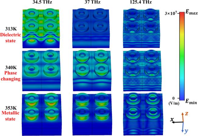
Figure 6. The electric field distribution of the absorption film. |
AlCuFe is a Dirac semimetal that can tune its Fermi energy (Ef) through doping and other means to change conductivity, making tunable optoelectronic devices [55, 56]. Figure 7(a) shows the absorption spectrum at 313 K. It can be seen that as Ef increases from 75 to 95 meV, the absorption spectrum undergoes a blue shift and exhibits a strong multi-band absorption response. When Ef is equal to 75 meV, the absorption film exhibits dual-band absorption, with absorption rates around 0.99. As Ef increases, more bands are excited until stable seven-band absorption occurs at 95 meV. So different Efs can be set according to different requirements to obtain multi-band absorption. At 353 K (figure 7(b)), due to the fact that VO2 is in the metallic state, the electromagnetic absorption of the absorption film mainly comes from electromagnetic coupling at the AlCuFe interface. Therefore, the high carrier mobility brought about by the increase in Ef enhances the electromagnetic absorption of AlCuFe, resulting in a shift to a higher frequency in the absorption spectrum and a more stable absorption rate.
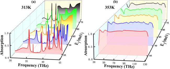
Figure 7. Absorption spectra of absorption film for different Ef: (a) the 30–45 THz band; (b) the 30–130 THz band. |
Figure 8(a) shows the absorption spectra of the absorbing film at 313 K for different H2. It can be seen that when H2 increases from 2.18 to 2.58 μm, the change in H2 will affect the guided-mode resonance coupling located in VO2, leading to the absorption spectrum of the absorbing film undergoing a red shift and exhibiting different multi-band absorption responses. Similarly, figure 8(c) shows the absorption spectrum of the absorption film at 313 K with different H3. It is evident that as H3 increases, affecting the electromagnetic coupling in AlCuFe, the absorption spectrum undergoes a blue shift. Based on this, we can stimulate different couplings to obtain the ideal absorption response according to particular requirements. For example, when H3 = 2.16 μm, the multi-band absorption at 40–45 THz will be strengthened, while when H3 = 2.76 μm, better quality absorption peaks will be observed in the front bands. This means that the absorption film is strongly tunable, and different physical parameters can be set according to different requirements in the sensing band. Figures 8(b) and (d) show the absorption spectra for different physical parameters at 353 K. It is obvious that the bandwidth absorption response of the absorption film is roughly the same under different parameters, which gives the absorption film a large processing tolerance in bandwidth absorption.
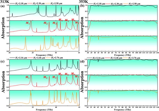
Figure 8. (a) Absorption spectra of different H2 at 313 K. (b) Absorption spectra for different H2 at 353 K. (c) Absorption spectra for different H3 at 313 K. (d) Absorption spectra for different H3 at 353 K. |
Multi-band absorption is commonly employed in optical sensing applications, emphasizing the significance of the absorption mode's sensing performance. In general, the refractive index sensitivity serves as the most direct indicator for evaluating the sensing performance of a device. As shown in figure 9(a), the absorption spectra under different background refractive indices show that the M5 response disappears with increase in the background refractive index. Therefore, when considering the refractive index sensitivity in this paper we will not discuss this mode, but mainly discuss other more stable absorption modes. The refractive index sensitivity S of each mode is defined as [57–59]
$\begin{eqnarray}S={\rm{\Delta }}\lambda /{\rm{\Delta }}n\end{eqnarray}$
where $\unicode{x02206}\lambda $ is the band in which the absorption peak shifts while $\unicode{x02206}n$ is the change in the background refractive index. Figure 9(b) shows the regression curve and mathematical equation for each absorption mode. It is obvious that the refractive index sensitivities of M1, M2, M3, M4, M6 and M7 are 3000, 1125, 1800, 750, 1275 and 900 GHz R−1 IU−1, respectively. This means that the absorption film has good sensing potential and an extremely high application value in fields such as biosensing.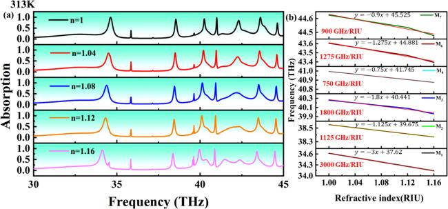
Figure 9. (a) Absorption spectra for different background refractive indices. (b) Sensitivity of M1–M7. |
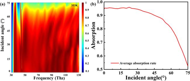
In the realm of electromagnetic absorption, such as IR stealth, the incidence angle tolerance is a vital criterion for assessing the efficacy of the absorption film [60, 61]. This implies that the absorption film must exhibit stable performance even at high incidence angles. The scanning spectra of the bandwidth response at different angles of incidence at 353 K are shown in figure10(a). It is worth noting that the absorption film exhibits a consistently high absorption rate before 40°. As the incident angle increases, defects appear in the absorption spectrum around 40 THz, but the absorption rate in other bands remains at around 0.8 even at an incident angle of 60°. Figure 10(b) depicts the average absorption rate within the 35–130 THz frequency band at various incidence angles. The results indicate that incidence angles below 45° yield an average absorption rate exceeding 0.9. However, for incidence angles surpassing 60°, the average absorption rate decreases below 0.8. Remarkably, at an incidence angle of 75°, the average absorption rate reaches approximately 0.5. This suggests that the thin film exhibits excellent tolerance for incident angles, maintaining its absorption efficiency even at large incident angles [62, 63]. Consequently, it holds significant potential for applications in fields such as electromagnetic shielding [64, 65].
Figure 10. (a) Scanning spectra at different incident angles. (b) Average absorption rate. |
Table 1 presents a compilation of the different types of absorption films that have been reported in recent years. Notably, references [16] and [17] highlight absorption films with multi-band/bandwidth absorption switching capabilities, while the remaining references focus on single-functional absorption films. These absorption films exhibit limitations such as single functionality, narrow absorption bandwidth and low refractive index sensitivity. The proposed absorption film in this paper stands out due to its ability to switch absorption responses, as well as its remarkably simple structure, tunability and sensitivity. These characteristics offer significant advantages in fields such as biosensing and IR stealth applications.
Table 1. Absorption films reported in recent years. |
| Absorption response | Tunability | Max. sensitivity (GHz R−1 IU−1) | Optimization | Reference |
|---|---|---|---|---|
| Single band | Temperature | – | – | [66] |
| Three-band absorption | Voltage/hybridization | 152.5 | – | [24] |
| Five-band absorption | – | 1370 | – | [32] |
| 10 THz bandwidth absorption | Voltage/hybridization | – | – | [27] |
| 16 THz bandwidth absorption | – | – | PSO algorithm | [67] |
| 100 THz bandwidth absorption | – | – | PSO algorithm | [68] |
| Dual-band/1 THz bandwidth absorption | Temperature, voltage | – | – | [18] |
| Single band/3.7 THz bandwidth absorption | Temperature, voltage | [19] | ||
| Seven-band/93 THz bandwidth absorption | Temperature, voltage/hybridization | 3000 | PSO algorithm | This paper |
Conclusion
This paper presents a novel intelligent absorption film that demonstrates dual-tunable ultra-wideband/narrowband switching capabilities. The film achieves multi-band absorption within the frequency range of 30–45 THz; it can achieve absorption with a bandwidth of 94 THz (with an absorption rate exceeding 0.9) within the range of 30–130 THz by controlling the temperature. The relative impedance of the absorption film aligns with the impedance matching theory, and its symmetrical structure results in strong polarization incoherence. The film can be tuned through various means, including doping/voltage, temperature and structural parameter adjustments. Furthermore, by adjusting the structural parameters, the absorption film can achieve diverse multi-band absorption responses within the sensing band, indicating strong tunability. Additionally, when the background refractive index is modified, we observed that most modes within the sensing band exhibit high sensitivity to refractive index changes. This characteristic renders the absorption film highly promising for applications in fields such as biomedicine, where excellent sensing performance is crucial. Moreover, the absorption film exhibits a wider bandwidth and higher absorption rate in the bandwidth absorption response while also demonstrating a certain level of insensitivity to incident angles. These properties make the absorption film a viable candidate for applications in fields such as biosensing and IR stealth.
Declaration of competing interest
The authors declare that they have no known competing financial interests or personal relationships that could have appeared to influence the work reported in this paper.