


Introduction
Terahertz waves are a type of electromagnetic wave characterized by frequencies ranging from 0.1 to 10 THz and corresponding wavelengths of 0.03–3 mm [1–5]. These waves possess notable attributes, such as low energy, strong penetration, and coherence, which contribute to their wide-ranging potential applications [6–10]. Despite the fact that the terahertz band is still a topic of ongoing research, it is a challenging area because most natural materials generally exhibit weak electromagnetic responses within this frequency range. Terahertz devices made from these natural materials have drawbacks, such as large volume and low efficiency, which have led to slower progress in this field [11, 12]. Nevertheless, the development of terahertz absorbers based on electromagnetic resonators, as pioneered by Landy et al in 2008 [13], has significantly accelerated research progress in this field. Since then, numerous terahertz absorbers with similar structures have been developed, showcasing attributes, such as simple design, high absorption rates, and thin profiles. These advancements have been pivotal in expediting the growth and exploration of terahertz absorbers. Terahertz absorbers have immense potential for various applications, including fingerprint detection [14, 15], biomedicine [16, 17], electromagnetic stealth [18, 19], sensing [20, 21], process control and monitoring [22], modulators [23, 24], communication [25], and coding [26]. However, most of the metamaterials currently used have poor performance, and devices designed based on them have a single function and lack adjustability. This limits the practical application of this device [27–32]. In the last few years, the discovery and advancement of materials, such as VO2 [33–35], graphene [36–39], and liquid crystals [40, 41], have opened up new possibilities for terahertz absorber design. These materials exhibit conductivity and dielectric properties that can be dynamically tuned by altering parameters, such as temperature, light, and electricity. This flexibility enables the development of terahertz absorbers with a wide absorption bandwidth, high absorption rates, and the ability to adapt their absorption properties. Consequently, designing absorbers with these characteristics has emerged as a crucial research area in the field of terahertz technology. The emergence of metamaterials has made all of these possible.
The conductivity of VO2 exhibits high sensitivity to fluctuations in temperature. At approximately 341 K, VO2 undergoes a reversible phase transition from an insulating state to a metallic state [42], resulting in a significant alteration in its conductivity. This characteristic enables the manipulation of the conductivity of VO2 by controlling temperature changes, consequently facilitating dynamic adjustments to the performance of terahertz devices. As a result, recent research efforts have been dedicated to exploring terahertz absorbers based on VO2, capitalizing on its unique properties to achieve dynamic modulation of device functions. In 2019, Bai et al [43] proposed a VO2 metamaterial-based design for a tunable broadband terahertz absorber, exhibiting an absorption capacity exceeding the threshold of 90% in a bandwidth of 1.25 THz. Concurrently, a reconfigurable bandwidth terahertz absorber reliant on an isotropic VO2 metasurface was proposed by Song et al [44], presenting an absorption rate transcending 90% within the 0.47–0.99 THz span. In 2020, Huang et al [45] manipulated a mixed pattern in designing a terahertz absorber that manifested an absorption rate that attained levels beyond 90% for terahertz waves existing in the frequency range of 1.85–4.3 THz. Despite the dynamic tunability of these designs, they predominantly possess complex structures, which makes them challenging to construct. In addition, they tend to exhibit confined absorption bandwidths and inferior absorption rates. Consequently, the move toward creating absorbers characterized by a broad bandwidth, superior absorption, dynamic tunability, and an uncomplicated structure is seen as a viable developmental tendency.
With this goal, this study proposes a terahertz device incorporating a three-layer structure of VO2–SiO2–Au. This device can respond to external temperature stimuli and quickly adjust its absorption capacity. It can actualize the shift between complete reflection and perfect absorption performance. Hence, it is known as a ‘temperature-controlled tunable metamaterial terahertz device'. The simulation results showed that the device exhibited a total reflection capability toward terahertz waves at 313 K. However, when the temperature was set to 353 K, the device showed outstanding absorption, ranging between ultrawideband intervals of 5.00–8.55 THz. Consequently, by manipulating the temperature, the functionality of the device can be flexibly and automatically adjusted. In this paper, we examine and interpret the reasons for the transformation in the absorption proficiency of devices from complete reflection to perfect absorption. The phase transition of VO2 was indirectly substantiated by generating an electric field diagram on the surface of the device. This study investigated the impact of the five key structural parameters on the absorption performance of the device. Ultimately, the device was found to be insensitive to polarization, exhibiting nearly identical absorption graphs in both transverse electric (TE) and transverse magnetic (TM) modes. In addition, almost no sensitivity was exhibited, preserving its performance over a wide angular range in both modes. The device developed in this study demonstrates broad potential for practical applications because of its reduced limitations. Its advantages make it a promising solution in domains, such as terahertz stealth, energy harvesting, and modulation, delivering an effective and viable plan for research in relevant domains.
Structure design and unit cell model
The design configuration of the terahertz device proposed in this study is illustrated in figure 1. Figures 1(a)–(c) correspond to the structural stereogram, overhead view, and lateral view of the structure, respectively. The complete framework of the device comprised three layers. The lowermost reflectance layer is composed of a thin Au film. The thickness of this film substantially surpasses the maximum skin depth of the terahertz wave in Au, ensuring zero transmission and blocking the passage of terahertz waves through the Au film [46]. The intermediate dielectric layer is composed of SiO2 with a dielectric constant of 2.13, so that the terahertz wave incident on the device is dissipated in it after multiple reflections [47]. The top resonant layer is composed of VO2, and its pattern is a circle with a cross in the middle. Our design is a subwavelength periodic array structure that extends infinitely in the x and y directions, as shown in figure 1(a). In the simulation experiment, we set periodic boundary conditions in the x and y directions, so only one periodic element can be taken, which greatly reduces the calculation time. In addition, we set up a perfect matching layer and reflection boundary conditions in the +z direction above the source to make our simulation results more realistic and reliable. Using the COMSOL simulation platform, the finite element method was used to optimize the structural parameters of the device. In parameter optimization, we adopted the principle of controlling variables, taking only one structural parameter as a variable at a time, simulating and calculating the absorption effect corresponding to different parameter values. The parameter value corresponding to the best absorption effect was the optimized parameter value. After the extensive simulation, the optimal geometric parameters were as follows: L = 35 μm, R = 15.5 μm, M = 24 μm, H = 4 μm, O = 0.05 μm, P = 7.5 μm, and Q = 10 μm.
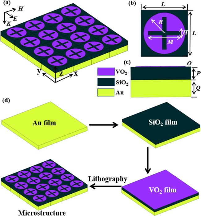
Figure 1. (a) Structural stereogram; (b) aerial view of the structure; (c) lateral view of the structure; (d) process flow diagram of the terahertz device. |
The manufacturing process of this device is shown in figure 1(d). First, ultrasound was used to clean the Si substrate with acetone, anhydrous ethanol, and deionized water. Then, a thin Au film with a thickness of 10 μm was generated on a Si substrate using magnetron sputtering. Next, an ion beam was used to generate a 7.5 μm thick SiO2 layer on the surface of the Au film. Next, magnetron sputtering was used to prepare a VO2 top layer with a thickness of 0.05 μm. Finally, the desired structure was obtained by lithography processes, such as exposure, development, plasma etching, and stripping.
Results and discussion
The absorption of the device under different temperature conditions was calculated using simulation software. Figure 2(a) shows that by controlling temperature alterations, the absorption capacity of the device can be adjusted with an adjustment range from 0 to 0.99. At a lower temperature (313 K), the device demonstrated total reflective properties throughout the entire band range. When the temperature was increased, the absorption rate correspondingly increased. Upon reaching 353 K, the absorption rate soared above 95% across the ultrawideband frequency of 4.6–8.6 THz, and it eclipsed 97.7% within the 5–8.55 THz frequency interval. Among them, the device absorption rate reached 99% in the range of 7.2–7.45 THz.
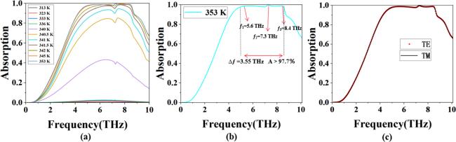
Figure 2. (a) Absorption of the device at different temperatures; (b) absorption rate of the device at T = 353 K; (c) spectrogram in TE and TM modes (T = 353 K). |
In addition, as shown in figure 2(c), the absorption effect of the device on terahertz wave is almost the same in the TE and TM modes, which signifies that the device engineered in this study is polarization insensitive, and this polarization independence is attributed to its high inherent symmetry. This geometric uniformity ensures that the characteristics of the device remain unaffected by the orientation of the electric field of the incident radiation [48].
The model absorption in this study can be expressed as [49]
$\begin{eqnarray}A\left(\omega \right)=1-R\left(\omega \right)-T\left(\omega \right),\end{eqnarray}$
where $R\left(\omega \right)$ is reflectivity, and $T\left(\omega \right)$ is transmissivity. Given that the thickness of the Au film at the base of the device greatly surpasses the maximum skin depth of terahertz waves in Au, the previous equation can be simplified as follows: $\begin{eqnarray}A\left(\omega \right)=1-R\left(\omega \right),\,\end{eqnarray}$
which indicates that the terahertz wave incident on the device will not penetrate the Au film.To investigate the transition of device performance from complete reflection to complete absorption, we used the Drude model on the COMSOL simulation platform to plot the surface electric field distribution of the device at different temperatures, as shown in figure 3. Figure 3(a) indicates that with an increase in temperature from 313 to 340 K, there was a slow increase in the intensity of the electric field. However, a significant surge in the electric field intensity from 106 to 107 V m−1 was observed when the temperature increased beyond 340 K. The reason for this was that the resonance layer on the device surface was composed of VO2, a material renowned for its phase-transformation attributes related to temperature [50]. Upon reaching a temperature of approximately 341 K, VO2 underwent a reversible phase transition, shifting from a monoclinic insulating phase to a tetragonal metallic phase [49], as depicted in figure 3(b). Before and after the phase change, the photoelectric properties of VO2 underwent a huge mutation [51]. In the phase-transition process, with an increase in temperature, the VO2 thin film first produced sporadic metal phase-transition points, and then the phase-transition region gradually expanded and finally became a piece [52]. Therefore, the insulating and metal phases existed simultaneously during the whole phase-transition process, and this composite system had a huge impact on the macro-dielectric properties of VO2 [53]. The thermally induced phase-transition property of VO2 made the designed device dynamically tunable. Moreover, the dielectric properties of VO2 underwent significant changes after the phase transition, resulting in a significant increase in the absorption rate of the device.
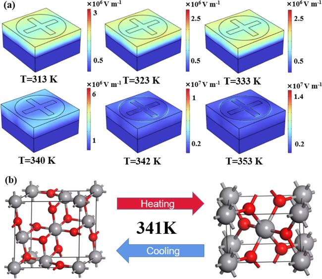
Figure 3. (a) Variation of electric field intensity distribution with increasing temperature (TE mode; ƒ = 7.3 THz; vertical incidence); (b) transition between monoclinic and rectangular crystal systems during the VO2 phase transition. |
With the aim of investigating the correlation between temperature and conductivity of VO2, the Bruggeman effective medium theory [54] is introduced in this paper, and the dielectric constant of the composite system is [55, 56]5 ) into equation (4 ), we obtained
$\begin{eqnarray}\begin{array}{l}{\varepsilon }_{C}=\displaystyle \frac{1}{4}\left\{{\varepsilon }_{D}\left(2-3\,{\rm{\unicode{x00192}}}\right)+{\varepsilon }_{M}\left(3\,{\rm{\unicode{x00192}}}-1\right)\right.\\ \left.+\,\sqrt{{\left[{\varepsilon }_{D}\left(2-3\,{\rm{\unicode{x00192}}}\right)+{\varepsilon }_{M}\left(3\,{\rm{\unicode{x00192}}}-1\right)\right]}^{2}+8{\varepsilon }_{D}{\varepsilon }_{M}}\right\}.\end{array}\end{eqnarray}$
In this context, $\unicode{x00192}$ represents the volume fraction of the metallic phase, ${\varepsilon }_{D}$ indicates the dielectric constant of the insulator phase, and ${\varepsilon }_{M}$ denotes the dielectric constant of the metallic phase. The insulating phase of VO2 can be perceived as a dielectric with a constant of ${\varepsilon }_{D}=9.$ As per the Drude model [57, 58], the dielectric constant ${\varepsilon }_{M}$ for the metal phase can be articulated as $\begin{eqnarray}{\varepsilon }_{M}\left(\omega \right)={\varepsilon }_{\infty }-\displaystyle \frac{{\omega }_{p}^{2}}{{\omega }^{2}+\tfrac{{\rm{i}}\omega }{\tau }}.\end{eqnarray}$
In this case, $\omega $ stands for the circular frequency of the terahertz wave, ${\varepsilon }_{\infty }$ embodies the high-frequency dielectric constant of VO2, $\tau =2.2$ fs designates the carrier collision time, and ${\omega }_{{\rm{p}}}$ refers to the plasma frequency, which can be stated as $\begin{eqnarray}{\omega }_{{\rm{p}}}=\sqrt{\displaystyle \frac{N{e}^{2}}{{\varepsilon }_{0}{m}^{* }}},\end{eqnarray}$
where $N$ represents the carrier concentration of the medium, ${\varepsilon }_{0}$ represents the permittivity of vacuum, and ${m}^{* }$ signifies the effective mass. By substituting equation ( $\begin{eqnarray}{\varepsilon }_{M}\left(\omega \right)={\varepsilon }_{\infty }-\displaystyle \frac{\tfrac{N{e}^{2}}{{\varepsilon }_{0}{m}^{* }}}{{\omega }^{2}+\tfrac{i\omega }{\tau }}.\end{eqnarray}$
For the VO2 film [59], ${\varepsilon }_{\infty }=9,$ ${\varepsilon }_{D}=9,$ $N=1.3\,\times {10}^{22}\,{{\rm{cm}}}^{-3},$ and ${m}^{* }=2{m}_{{\rm{e}}}.$The Boltzmann function [60] was also incorporated to depict the correlation between the volume fraction $\unicode{x00192}$ of the VO2 metallic phase and the temperature $T:$ 3 ), (6 ), and (7 ) into equation (8 ) and using Excel for data calculation, the obtained data were plotted using Origin to obtain the correlation between the conductivity of VO2 and temperature, as shown in figure 4, where the horizontal axis represents the temperature, and the vertical axis represents the logarithmic value of conductivity. This diagram provides an understanding of how temperature changes affect the conductivity of the VO2 components in devices. Figure 4 clearly shows that when the temperature increased to approximately 341 K, a significant shift in the conductivity of VO2 occurred, increasing up to three orders of magnitude. At 313 K, the conductivity remained at 130 S m−1. Upon increasing the temperature to 345 K, the conductivity increased to an impressive 200 000 S m−1. In the former scenario, the device functioned like an insulator–dielectric–metal structure, which can almost entirely reflect the incident terahertz wave, thereby achieving a high reflective efficiency. In the latter case, the device can be perceived as a metal–dielectric–metal structure that is capable of achieving high absorption at particular terahertz wave frequencies. This is because the first structure did not form a resonant cavity, whereas the second structure formed a resonant cavity, which can resonate with terahertz waves at a specific frequency and produce high absorption [62]. Therefore, the absorption effect of the device can be adjusted by controlling the change in temperature to realize the conversion of the device functions.
$\begin{eqnarray}{\rm{\unicode{x00192}}}\left(T\right)={{\rm{\unicode{x00192}}}}_{\max }\left(1-\displaystyle \frac{1}{1+{e}^{\tfrac{T-{T}_{0}}{{\rm{\Delta }}T}}}\right),\end{eqnarray}$
where ${\unicode{x00192}}_{{\rm{\max }}}$ represents the maximum volume fraction of the VO2 metallic phase at peak temperatures, and its value was 0.95. The value of ${T}_{0}$ represents the critical phase-transition temperature of VO2, which occurred at 341.15 K while heating and 336.15 K during cooling. ${\rm{\Delta }}T$ is the transition temperature, which was 2 K. Simultaneously, the conductivity and dielectric constant of the material can be denoted by [61] $\begin{eqnarray}\sigma =-{\rm{i}}{\varepsilon }_{0}\omega \left({\varepsilon }_{c}-1\right).\end{eqnarray}$
By substituting equations (To examine the broadband absorption mechanism of the device at T = 345 K, its electric field distribution at three distinct absorption peaks (ƒ1, ƒ2, and ƒ3), as illustrated in figure 5, was plotted. This provides a visual representation of the electric field distribution of the device under multiple absorption peak conditions. From figures 5(a), (c), (d), and (f), it is apparent that the electromagnetic field was polarized along the Y direction, with a relatively strong distribution of the electrical field intensity in the polarization direction. This field intensity was mainly distributed in the upper and lower parts of the disc and along the edge of the cross structure, indicating a symmetrical distribution around the Y axis. This local intensification of the electric field was a result of frequency synchronization between the VO2 resonant structure and the terahertz wave. This alignment induced local surface plasmon resonance [63], culminating in complete absorption [64]. When resonance occurred, the incident terahertz wave continuously reflected between the VO2 film structure and the Au substrate and gradually dissipated in the dielectric layer, forming nearly 100% perfect absorption. Furthermore, the electric field distributions at the frequencies of ƒ1 and ƒ3 showed a striking resemblance, implying that the two resonance modes were the same or bear a likeness. This similarity pertains to the resonance structure formed by the slanted edge of the disc and the edge of the cross structure. The polarization direction of the electromagnetic field can be observed to be along the Y direction in figures 5(b) and (e). However, the difference lies in the distribution of the electric field, which is centered on the Y axis. This suggests that the perfect absorption at the frequency of ƒ2 resulted from another resonant mode, associated with the resonant structure formed by the top and bottom sides of the disc and the intersection of the cross structure.
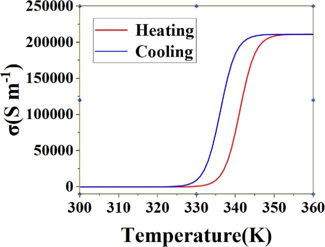
Figure 4. Relationship between the conductivity of VO2 and temperature. |
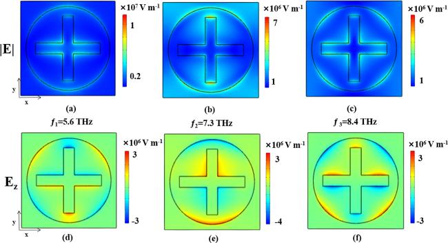
Figure 5. Electric field distribution of the device under absorption peak. |
The preceding discussion pertains only to absorption in an ideal scenario. In reality, the precision of the manufacturing process may also influence the absorption effectiveness of the device. To investigate the specific effects of different structural parameters on the absorption rate of the device, we used the control variable method to simulate and calculate the absorption rate of the device under five different structural parameters, which are plotted in figure 6. As shown in figures 6(a)–(c), the most evident structural parameter influencing the VO2 pattern was the radius R of the VO2 disc. As R increased, the absorption bandwidth significantly expanded. The perfect absorption effect occurred when R = 15.5 μm. When R = 17.5 μm, the absorption rate stayed above 90%, thereby covering half the bandwidth of the terahertz band. When the length M of the rectangle within the VO2 disc varied within the range of 22–26 μm, the absorption bandwidth remained virtually constant. As the width H of the rectangle within the VO2 disc increased, the absorption bandwidth slightly diminished. This occurred as the original resonant structure became disrupted with the alteration in VO2 size, which cannot match the frequency of the terahertz wave at this juncture. Moreover, as shown in figures 6(d) and (e), the absorption bandwidth experienced minor changes with an increase in the SiO2 dielectric layer thickness P, but the absorption range exhibited a prominent redshift. As the thickness O of the VO2 disc increased, there was a slight expansion in the absorption bandwidth, while the absorption effect remained stable. The aforementioned analysis offers guidance and insights for selecting the appropriate device parameters for practical applications.
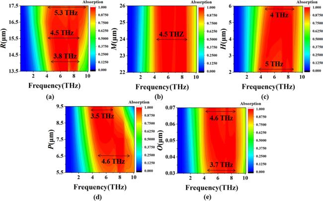
Figure 6. Scanning diagram of the structural parameters of the device at 353 K: (a) VO2 disc radius; (b) length of the rectangle in the VO2 disc; (c) width of the rectangle in the VO2 disc; (d) thickness of the SiO2 dielectric layer; (e) thickness of the VO2 disc. |
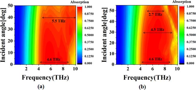
In practical applications, terahertz waves do not always interact with devices in a vertical way; therefore, devices are required to have a certain wide-angle characteristic so that terahertz waves incident at a certain angle can be better absorbed. Through simulated calculations, it was determined that the device designed in this study exhibits high angle insensitivity, as shown in figure 7. In this context, figures 7(a) and (b) illustrate the behavior of terahertz wave absorption at various incident angles when the device operates in the TE and TM modes, respectively. As shown in figure 7(a), with an increasing angle of incidence, there is a noticeable expansion in the absorption bandwidth of the device in the TE mode. At an incident angle of 0°, the absorption bandwidth of the device in the TE mode was 4.6 THz. As the angle increased to 40°, the absorption bandwidth expanded to 5.5 THz. However, with a further increase in the angle, the absorption effect gradually diminished due to the substantial decrease in the terahertz wave energy reaching the device surface. This led to a decrease in resonance unit excitation, which decreased the absorption rate [65, 66]. In figure 7(b), it can be observed that the absorption bandwidth of the device in the TM mode decreased gradually as the incident angle increased. Within the range of 0°–30°, the absorption bandwidth remained relatively constant at approximately 4.6 THz. However, beyond an incident angle of 30°, the absorption bandwidth significantly decreased. At an incident angle of 50°, the absorption bandwidth was measured to be 2.7 THz. In summary, the absorption effect of the device on terahertz waves diminishes gradually as the angle of incidence increases in both the TE and TM modes. Despite this, the device can maintain excellent performance over a wide range of incident angles. The angle insensitivity of the device greatly increases its application scenarios, reduces the limitations of using the device, and allows the device to still be used in many scenarios, which gives the device performance a certain degree of stability.
Figure 7. Terahertz wave absorption of the device at different incident angles: (a) TE mode, T = 353 K; (b) TM mode, T = 353 K. |
To reflect the absorption capacity of the device proposed in this study, we searched for terahertz absorbers with similar structures for comparison, as shown in table 1. Compared to the first four devices in table 1, the device engineered in this study has a simple three-layer structure and is easier to manufacture, providing an edge over other devices. At the same time, compared with the last three devices, the absorption efficiency of the device was very high. When T = 353 K, the absorption bandwidth reached 3.55 THz, and the absorption efficiency exceeded 97.7%. Both the absorption bandwidth and absorption rate are much higher than those of other similar broadband terahertz absorbers listed in table 1 [65–71]. Overall, the device designed in this study has significant features, such as a simple structure, wide absorption bandwidth, and high absorption rate, compared to other devices.
Table 1. Performance comparison of similar broadband terahertz absorbers. |
Conclusions
In this study, a wideband, high-absorption, dynamically tunable terahertz device with a simple structure was developed. The device was composed of a VO2 top layer, SiO2 dielectric layer, and Au bottom layer structure, thereby facilitating easy fabrication. The results showed that the device completely reflected the terahertz waves at 313 K. At 353 K, the device demonstrated an absorption rate of more than 95% within the ultrawideband range of 4.6–8.6 THz. Furthermore, within a wide range of 5–8.55 THz, the absorption rate reached 97.7%. These high absorption rates indicate an almost perfect absorption of terahertz waves by the device. Additionally, owing to the high symmetry of the device, it is insensitive to both the polarization and the angle of incidence. In both the TE and TM modes, the device maintained commendable performance over a wide range of angles. These advantages suggest that the device developed in this study has considerable application potential in fields such as terahertz stealth, energy harvesting, and modulation.
Declaration of competing interest
The authors declare that they have no known competing financial interests or personal relationships that could have influenced the study reported in this paper.