


1. Introduction
Due to efficient algorithms [1–3] and secure communication [4, 5], quantum information processing has shown great advantages over classical information processing. Quantum logic gates play a critical role in quantum computation and quantum information processing [6]. It has been proved that any unitary operation for quantum computing can be realized by combining CNOT gates and single-qubit operations [7, 8]. In past decades, many schemes have been proposed to realize CNOT gates both in theory and experiment by using various quantum systems, such as atoms [9–11], ion traps [12], quantum dots [13–16], diamond nitrogen-vacancy centers [17–20], superconducting circuits [21, 22] and nuclear magnetic resonance [23–26].
In quantum computation, due to their remarkable transmission speed and robustness against the environment noise, photons usually play the role of flying qubits. In fact, a single photon has multiple DOFs to be encoded on, such as polarization, spatial mode, and frequency, which enhances the information-carrying capacity and improves the quality of the long-distance quantum computing [27–29]. Therefore, in recent years, hyperparallel photonic quantum computing has been proposed with encoding qubits on two or more DOFs of photons [30–35]. For example, Ren et al proposed some schemes for realizing the hyperparallel CNOT gate, CPF gate and Toffoli gate acting on the polarization and spatial DOFs [36, 37]. Based on the giant optical circular birefringence induced by the double-sided quantum-dot-cavity system, Wang et al constructed a deterministic hybrid hyper-CNOT gate [38]. Then, resorting to the cavity-assisted interaction, Du et al constructed some schemes for realizing hybrid hyper-CNOT gates on the two-photon system in both the polarization and spatial-mode DOFs [39]. Utilizing multiple DOFs, these hyperparallel quantum gates can improve the calculation speed, expand the quantum channel capacity, and reduce the noise caused by photonic dissipation. Moreover, hyperparallel photonic quantum gates have vital applications in hyperentanglement generation [40, 41], hyperentanglement concentration [42, 43], and hyperentanglement purification [44–46].
Different from previous schemes, our hyper-CNOT gates are based on waveguide quantum electrodynamics (QED), which has emerged as an exciting frontier in quantum information science [47–58]. A waveguide system is coupled with nearby atoms or embedded artificial atoms through the continuous electromagnetic modes with a large bandwidth. In fact, many physical systems can act as waveguide platforms, such as optical nanofibers [59–62], photonic crystal waveguides [63–66], plasmonic nanowires [67], superconducting transmission lines [68, 69] and so on. Interestingly, in the resonant case, a two-level quantum emitter coupled with a waveguide can completely reflect an input photon, which reveals that the quantum emitter behaves as a photon mirror [70, 71]. Based on this model, Li et al constructed a robust-fidelity atom-photon entangling gate [72], which can also be applied to time bin- or polarization-encoded photonic qubits. In their schemes, faulty interactions between photons and quantum emitters can be filtered out and discarded, rendering an error-heralding mechanism. In past decades, tremendous progress has been made in waveguide QED both in theory and experiment [73–82], which paves the way for constructing quantum gates in waveguide systems.
In this paper, with the scattering properties of photons off quantum emitters in 1D waveguides, we present three schemes for constructing heralded four-qubit hyper-CNOT gates in two-photon systems. The qubits are encoded on both the polarization and spatial-mode DOFs of photons. In our protocols, the wrong scattering events between auxiliary emitters and photons in 1D waveguides, caused by frequency detunings, weak couplings and decay into unwanted modes, can be transformed into heralded photon losses. In other words, faulty scattering processes in our three protocols for hyper-CNOT gates can be picked out and discarded. Thus, our schemes work in a heralded manner, which is a highly advantageous feature for quantum computation or communication. With great progress in interfacing quantum emitters with nanophotonic waveguides, our schemes provide an effective avenue for implementing quantum gates and may have potential applications in quantum information processing.
The paper is organized as follows. In section 2 , we review the photon scattering off single emitters coupled to a 1D waveguide and present a heralded setup for realizing a Z gate on a quantum emitter. Then, in section 3 , we propose three heralded schemes for constructing four-qubit hyper-CNOT gates in two-photon systems. Finally, in section 4 , we discuss the fidelities of our three schemes in realistic emitter-waveguide systems and summarize our work.
2. Photon scattering in 1D waveguides
Here, we consider a quantum system that a two-level emitter is coupled to a 1D waveguide through electromagnetic modes, as shown in figure 1(a). The quantum emitter has two electronic levels, i.e., the ground and excited states ∣g⟩ and ∣e⟩ with frequency difference ${\omega }_{{}_{a}}$. We focus on the case that the resonance frequency ${\omega }_{{}_{a}}$ is away from the cut-off frequency of the waveguide modes, and the Hamiltonian of the quantum system in real space can be written as (ℏ = 1) [70, 83]
$\begin{eqnarray}\begin{array}{l}H=\left({\omega }_{{}_{a}}-\displaystyle \frac{{\rm{i}}\gamma {{\prime} }_{e}}{2}\right){\sigma }_{{ee}}+{\rm{i}}{v}_{g}\\ \,\,\times \,\displaystyle \int {\rm{d}}x\left[{c}_{{}_{L}}^{\dagger }(x)\displaystyle \frac{\partial {c}_{{}_{L}}(x)}{\partial x}-{c}_{{}_{R}}^{\dagger }(x)\displaystyle \frac{\partial {c}_{{}_{R}}(x)}{\partial x}\right]\\ \,\,+V\displaystyle \int {\rm{d}}x\delta (x)\left\{{\sigma }_{e{\rm{g}}}[{c}_{{}_{R}}(x)+{c}_{{}_{L}}(x)]+{\rm{H}}.{\rm{c}}.\right\}.\end{array}\end{eqnarray}$
Here, $\gamma {{\prime} }_{e}$ represents the decay rate of the excited state ∣e⟩ absent the waveguide, and vg denotes the group velocity of photons in the 1D waveguide. ${c}_{{}_{R}}$ and ${c}_{{}_{L}}$ (${c}_{{}_{R}}^{\dagger }$ and ${c}_{{}_{L}}^{\dagger }$) are the annihilation (creation) operators of right- and left-propagating fields, respectively. V denotes the coupling strength between the quantum emitter and the waveguide, where we assume it is the same for all electromagnetic modes. σαβ = ∣α⟩⟨β∣ is the operator of the two-level quantum emitter, where α, β = g, e.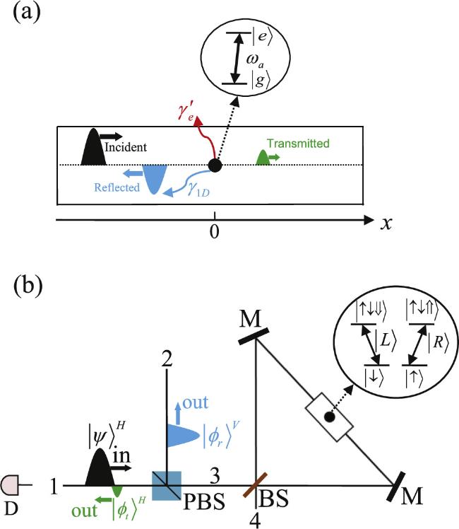
Figure 1. (a) Schematic diagram for the photon scattering by a two-level quantum emitter (the black dot) coupled to a 1D waveguide (the rectangle). A photon (black wave packet) is injected from the left to scatter with the emitter, which creates a reflected component (blue wave packet) and a transmitted component (green wave packet). (b) The scheme for realizing a heralded Z gate on an emitter in a 1D waveguide. Polarizing beam splitter (PBS) is a polarizing beam splitter, which transmits the photon in the horizontal polarization state ∣H⟩ and reflects the photon in the vertical polarization state ∣V⟩. D is a single-photon detector, beam splitter (BS) represents a 50:50 beam splitter, and M is a fully reflected mirror. The circular inset shows the energy level transitions of a negatively charged quantum dot chosen as the emitter. |
As shown in figure 1(a), a photon with energy Ek = kvg is injected from the left (k denotes the wave vector), and the emitter is initially prepared in the ground state ∣g⟩. By solving the eigenvalue equation, we can get the reflection amplitude r of the input photon as [71]2 ) shows that the reflection amplitude r ≈ − 1 when Δ = 0 and P → ∞ . In such case, we can get t = 0 and the two-level emitter acts as a quantum mirror, which imprints a π-phase shift in the reflected part of the photon [71]. However, when the quantum emitter is decoupled from the waveguide, the input photon goes through the emitter with nothing changed.
$\begin{eqnarray}r=-\displaystyle \frac{1}{1+1/P-2{\rm{i}}{\rm{\Delta }}/{\gamma }_{{}_{1D}}}.\end{eqnarray}$
Here, $P={\gamma }_{{}_{1D}}/\gamma {{\prime} }_{e}$ denotes the Purcell factor, and ${\gamma }_{{}_{1D}}=4\pi {V}^{2}/{v}_{g}$ is the decay rate of the quantum emitter into the waveguide modes. ${\rm{\Delta }}={\omega }_{\mathrm{in}}-{\omega }_{{}_{a}}$ represents the frequency detuning between the input photon and the emitter transition, with ωin being the frequency of the incident photon. The transmission amplitude t of the photon can be given by t = 1 + r. Equation (With the above scattering property in a 1D waveguide, a heralded Z gate on an emitter can be realized, as shown in figure 1(b). Here, the emitter has four energy levels, which can be implemented by a singly charged self-assembled InGaAs/GaAs quantum dot in experiment [84–86]. In detail, the optical transition ∣ ↑ ⟩ ↔ ∣ ↑ ↓ ⇑ ⟩ (∣ ↓ ⟩ ↔ ∣ ↑ ↓ ⇓ ⟩) can be driven by the absorption or emission of a right (left)-handed circular polarized photon ∣R⟩ (∣L⟩). In the experiment, for a quantum dot coupled to 1D waveguides, the scattering rule shown in figure 1(b) is imperfect because of the heavy-light hole mixing. That is, the cross transitions also exist in a practical system. However, the unwanted cross transitions can be strongly suppressed by adopting appropriate types of quantum dots and designing the direction of the external magnetic field [85]. In the following, for simplicity, we write the two degenerate ground states as: ∣ ↑ ⟩ = ∣g+⟩, ∣ ↓ ⟩ = ∣g−⟩. The photon scattering rules for the four-level emitter can be written as:
$\begin{eqnarray}\begin{array}{l}| {{\rm{g}}}_{+}\rangle | \psi \rangle | R\rangle \to | {{\rm{g}}}_{+}\rangle | \phi \rangle | R\rangle ,\\ | {{\rm{g}}}_{+}\rangle | \psi \rangle | L\rangle \to | {{\rm{g}}}_{+}\rangle | \psi \rangle | L\rangle ,\\ | {{\rm{g}}}_{-}\rangle | \psi \rangle | R\rangle \to | {{\rm{g}}}_{-}\rangle | \psi \rangle | R\rangle ,\\ | {{\rm{g}}}_{-}\rangle | \psi \rangle | L\rangle \to | {{\rm{g}}}_{-}\rangle | \phi \rangle | L\rangle .\end{array}\end{eqnarray}$
Here, ∣ψ⟩ and ∣φ⟩ are the spatial wave functions of the input photon and photon component in the waveguide after the scattering, respectively. In detail, ∣φ⟩ = ∣φr⟩ + ∣φt⟩, where ∣φr⟩ = r∣ψ⟩ and ∣φt⟩ = t∣ψ⟩ denote the spatial wave functions of the reflected and transmitted photon parts, respectively.As shown in figure 1(b), when the input photon is in the horizontal linear-polarization state $| H\rangle =(| R\rangle +| L\rangle )/\sqrt{2}$, the photon scattering rules can be written as:4 ) shows that the scattering process generates a new photon component, i.e., the vertical linear-polarization photon. More importantly, when the emitter is initially prepared in the state ∣g−⟩, a π-phase shift is imprinted on the emitter for the photon component ∣V⟩. This phase shift is the basis of the heralded Z gate on an emitter shown in figure 1(b). In detail, the emitter is initially prepared in the state ∣g+⟩ or ∣g−⟩, and a photon with the spatial state ∣ψ⟩ and polarization state ∣H⟩ is injected into the protocol from port 1. It transmits through the polarizing beam splitter (PBS) directly and then is split by the 50:50 beam splitter (BS) into two parts to scatter with the four-level emitter independently. Here, the PBS transmits the photon in the horizontal polarization state ∣H⟩ and reflects the photon in the vertical polarization state ∣V⟩, and the 50:50 BS performs a Hadamard operation on the spatial modes of the photon. After that, the two photon parts interfere with each other at the BS and quit the triangular scattering structure from port 3. Finally, the photon travels back to PBS, and the photon component in state ∣H⟩ (∣V⟩) exits from port 1 (2). The above scattering processes can be summarized as:7 ) evolves into
$\begin{eqnarray}\begin{array}{l}| {{\rm{g}}}_{+}\rangle | \psi \rangle | H\rangle \to | {{\rm{g}}}_{+}\rangle (| {\phi }_{t}\rangle | H\rangle +| {\phi }_{r}\rangle | V\rangle ),\\ | {{\rm{g}}}_{-}\rangle | \psi \rangle | H\rangle \to | {{\rm{g}}}_{-}\rangle (| {\phi }_{t}\rangle | H\rangle -| {\phi }_{r}\rangle | V\rangle ),\end{array}\end{eqnarray}$
where $| V\rangle =(| R\rangle -| L\rangle )/\sqrt{2}$ represents the vertical linear-polarization state. Equation ( $\begin{eqnarray}| {{\rm{g}}}_{\pm }\rangle | \psi \rangle | H{\rangle }^{{}^{1}}\to | {{\rm{g}}}_{\pm }\rangle | {\phi }_{t}\rangle | H{\rangle }^{{}^{1}}\pm | {{\rm{g}}}_{\pm }\rangle | {\phi }_{r}\rangle | V{\rangle }^{{}^{2}},\end{eqnarray}$
where the superscripts 1 and 2 denote the ports shown in figure 1(b). For a realistic emitter-waveguide system, ∣φt⟩ ≠ 0 and the single-photon detector in port 1 clicks, meaning that faulty scattering events occur in the setup. Note that, due to the destructive quantum interference, no photon quits from port 4. Similarly, when the input photon is in the vertical polarization state ∣V⟩ (not shown in figure 1(b)), we can obtain the corresponding evolution $\begin{eqnarray}| {{\rm{g}}}_{\pm }\rangle | \psi \rangle | V{\rangle }^{{}^{2}}\to | {{\rm{g}}}_{\pm }\rangle | {\phi }_{t}\rangle | V{\rangle }^{{}^{2}}\pm | {{\rm{g}}}_{\pm }\rangle | {\phi }_{r}\rangle | H{\rangle }^{{}^{1}}.\end{eqnarray}$
Discarding the faulty scattering events with unchanged photon polarization in the two cases, we can get $\begin{eqnarray}\begin{array}{l}| {{\rm{g}}}_{\pm }\rangle | \psi \rangle | H\rangle \to \pm | {{\rm{g}}}_{\pm }\rangle | {\phi }_{r}\rangle | V\rangle ,\\ | {{\rm{g}}}_{\pm }\rangle | \psi \rangle | V\rangle \to \pm | {{\rm{g}}}_{\pm }\rangle | {\phi }_{r}\rangle | H\rangle .\end{array}\end{eqnarray}$
In particular, for perfect emitter-waveguide systems, i.e., Δ = 0 and P → ∞ , we can easily get ∣φr⟩ = − ∣ψ⟩ and equation ( $\begin{eqnarray}\begin{array}{l}| {{\rm{g}}}_{\pm }\rangle | \psi \rangle | H\rangle \to \mp | {{\rm{g}}}_{\pm }| \psi \rangle \rangle | V\rangle ,\\ | {{\rm{g}}}_{\pm }\rangle | \psi \rangle | V\rangle \to \mp | {{\rm{g}}}_{\pm }\rangle | \psi \rangle | H\rangle .\end{array}\end{eqnarray}$
While, for practical emitter-waveguide systems, P is finite and ∣φr⟩ ≠ − ∣ψ⟩. In such case, the photon scattering may contain faulty events, which correspond to the photon output with unchanged polarization state. The faulty scattering events can be discarded by polarization filtering. Thus, the protocol for realizing the Z gate on an emitter shown in figure 1(b) works in a heralded manner.3. Three types of photonic hyper-CNOT gates
In this section, we present three heralded schemes for constructing hybrid hyper-CNOT gates on a two-photon system assisted by photon scattering in 1D waveguides. In detail, with the polarization and the spatial-mode DOFs, the two photons constitute a four-qubit system, where two qubits act as control qubits to flip the other two, respectively. In this section, we only give the evolutions of the system with perfect scattering events (i.e., equation (8 )), and the qualities of our protocols with realistic emitter-waveguide systems will be discussed in section 4 .
In the schemes, we assume that the two auxiliary emitters in 1D waveguides are initially both prepared in $| {{\rm{\Psi }}}_{{e}_{i}}\rangle \,=\tfrac{1}{\sqrt{2}}{(| 0\rangle +| 1\rangle )}_{i}$ (i = 1, 2). The photons A and B are initially prepared in arbitrary superposition states
$\begin{eqnarray}\begin{array}{rcl}| {{\rm{\Psi }}}_{A}\rangle & = & {\left({\alpha }_{1}| H\rangle +{\beta }_{1}| V\rangle \right)}_{A}\otimes ({\gamma }_{1}| {a}_{1}\rangle +{\delta }_{1}| {a}_{2}\rangle ),\\ | {{\rm{\Psi }}}_{B}\rangle & = & {\left({\alpha }_{2}| H\rangle +{\beta }_{2}| V\rangle \right)}_{B}\otimes ({\gamma }_{2}| {b}_{1}\rangle +{\delta }_{2}| {b}_{2}\rangle ),\end{array}\end{eqnarray}$
where ∣a1⟩ (∣b1⟩) and ∣a2⟩ (∣b2⟩) denote the two spatial modes of photon A (B), respectively. The coefficients satisfy ∣αi∣ + ∣βi∣2 = ∣γi∣2 + ∣δi∣2 = 1 (i = 1, 2).3.1. Hyper-CNOT gate type I
The hyper-CNOT gate type I can implement the function that the spatial modes of the photons A and B simultaneously control the polarization states of the photons B and A, respectively. As shown in figures 2(a)–(b), M1-ei and M2-ei represent two different modules of scattering processes. In M1-ei, only the photon part in state ∣V⟩ scatters with the emitter ei confined in the 1D waveguide. While, in M2-ei, both the ∣H⟩ and ∣V⟩ components of the photon interact with the emitter ei in the 1D waveguide, which occur in two independent paths. For both M1-ei and M2-ei, the photon part participated in scattering events goes through a quarter-wave plate (QWP), which flips the polarization states of the photon (∣H⟩ ⇌ ∣V⟩). With the two modules M1-ei and M2-ei, we construct hyper-CNOT gate type I, as shown in figure 2(c).
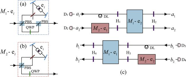
Figure 2. (a) and (b) are two different modules of interactions between a photon and the emitter ei (i = 1, 2). QWP represents a quarter-wave plate to flip the polarization state of a photon (∣H⟩ ⇌ ∣V⟩). (c) Schematic setup for realizing hyper-CNOT gate type I. Hj (j = 1, 2, 3, 4) denotes a half-wave plate to perform a Hadamard operation on the polarization states of a photon. DL is a time-delay device to guarantee the photon parts in different spatial paths to arrive at H1 or H3 simultaneously. Di (i = 1, 2, 3, 4) is a single-photon detector. |
Initially, the state of the whole system containing two photons (A and B) and two auxiliary emitters (e1 and e2) is14 ), one can see that the spatial modes of the photons A and B simultaneously control the polarization states of the photons B and A, respectively. When the measurement of the emitter e1 (e2) is ∣1⟩1 (∣1⟩2), an operation ${\sigma }_{{}^{Z}}^{{}_{S}}=| {a}_{1}\rangle \langle {a}_{1}| -| {a}_{2}\rangle \langle {a}_{2}| $ (${\sigma }_{{}^{X}}^{{}_{P}}=| H\rangle \langle V| +| V\rangle \langle H| $) needs to be performed on photon A. Then, we can also get the state ∣$\Psi$4⟩. Thus, the quantum circuit shown in figure 2(c) can realize the hyper-CNOT gate type I on a two-photon system.
$\begin{eqnarray}| {{\rm{\Psi }}}_{0}\rangle =| {{\rm{\Psi }}}_{A}\rangle \otimes | {{\rm{\Psi }}}_{B}\rangle \otimes | {{\rm{\Psi }}}_{{e}_{1}}\rangle \otimes | {{\rm{\Psi }}}_{{e}_{2}}\rangle .\end{eqnarray}$
We describe the principle of the quantum circuit in detail as follows. First, the photon A enters the circuit from the left. In detail, the photon A in spatial mode ∣a2⟩ passes through the module M2-e1, and immediately a Hadamard operation is performed on the emitter e1. Using H1, we also apply a Hadamard operation on the polarization states of photon A in both ∣a1⟩ and ∣a2⟩. After that, the state of the whole system evolves into $\begin{eqnarray}\begin{array}{rcl}| {{\rm{\Psi }}}_{1}\rangle & = & \displaystyle \frac{1}{\sqrt{2}}[{\alpha }_{1}{\left(| H\rangle +| V\rangle \right)}_{A}+{\beta }_{1}{\left(| H\rangle -| V\rangle \right)}_{A}]\\ & & \otimes ({\gamma }_{1}| {a}_{1}\rangle | 0{\rangle }_{1}+{\delta }_{1}| {a}_{2}\rangle | 1{\rangle }_{1})\otimes | {{\rm{\Psi }}}_{B}\rangle \otimes | {{\rm{\Psi }}}_{{e}_{2}}\rangle .\ \ \ \ \ \ \ \ \end{array}\end{eqnarray}$
Second, the photon A in both spatial modes ∣a1⟩ and ∣a2⟩ travels through M1-e2 and H2 successively. Note that, after the module M1-e2, a Hadamard operation is immediately performed on the emitter e2. After the above processes, the state of the system becomes $\begin{eqnarray}\begin{array}{rcl}| {{\rm{\Psi }}}_{2}\rangle & = & \displaystyle \frac{1}{2}| {{\rm{\Psi }}}_{B}\rangle \otimes ({\gamma }_{1}| {a}_{1}\rangle | 0{\rangle }_{1}+{\delta }_{1}| {a}_{2}\rangle | 1{\rangle }_{1})\\ & & \otimes [({\alpha }_{1}+{\beta }_{1}){\left(| H\rangle +| V\rangle \right)}_{A}| 0{\rangle }_{2}\\ & & \,+({\alpha }_{1}-{\beta }_{1}){\left(| H\rangle -| V\rangle \right)}_{A}| 1{\rangle }_{2}].\end{array}\end{eqnarray}$
Then, photon B enters the circuit from the right. Similar to photon A, photon B passes through M2-e2, H3, M1-e1, and H4, sequentially. Note that, after the module M2-e2 (M1-e1), a Hadamard operation is performed on the emitter e2 (e1). For perfect scattering events, i.e., no detector clicks, the state of the system becomes $\begin{eqnarray}\begin{array}{rcl}| {{\rm{\Psi }}}_{3}\rangle & = & \displaystyle \frac{1}{2}\{[{\gamma }_{1}| {a}_{1}\rangle {\left({\alpha }_{2}| H\rangle +{\beta }_{2}| V\rangle \right)}_{B}\\ & & +{\delta }_{1}| {a}_{2}\rangle {\left({\alpha }_{2}| V\rangle +{\beta }_{2}| H\rangle \right)}_{B}]| 0{\rangle }_{1}\\ & & +[{\gamma }_{1}| {a}_{1}\rangle {\left({\alpha }_{2}| H\rangle +{\beta }_{2}| V\rangle \right)}_{B}\\ & & -{\delta }_{1}| {a}_{2}\rangle {\left({\alpha }_{2}| V\rangle +{\beta }_{2}| H\rangle \right)}_{B}]| 1{\rangle }_{1}\}\\ & & \otimes \{[{\gamma }_{2}| {b}_{1}\rangle {\left({\alpha }_{1}| H\rangle +{\beta }_{1}| V\rangle \right)}_{A}\\ & & +{\delta }_{2}| {b}_{2}\rangle {\left({\alpha }_{1}| V\rangle +{\beta }_{1}| H\rangle \right)}_{A}]| 0{\rangle }_{2}\\ & & +[{\gamma }_{2}| {b}_{1}\rangle {\left({\alpha }_{1}| V\rangle +{\beta }_{1}| H\rangle \right)}_{A}\\ & & +{\delta }_{2}| {b}_{2}\rangle {\left({\alpha }_{1}| H\rangle +{\beta }_{1}| V\rangle \right)}_{A}]| 1{\rangle }_{2}\}.\end{array}\end{eqnarray}$
Finally, we need to measure the states of the auxiliary emitters e1 and e2 under the orthogonal basis {∣0⟩, ∣1⟩}. If the result is ∣0⟩1 and ∣0⟩2, the state of the two-photon system collapses into $\begin{eqnarray}\begin{array}{rcl}| {{\rm{\Psi }}}_{4}\rangle & = & [{\gamma }_{1}| {a}_{1}\rangle {\left({\alpha }_{2}| H\rangle +{\beta }_{2}| V\rangle \right)}_{B}\\ & & +{\delta }_{1}| {a}_{2}\rangle {\left({\alpha }_{2}| V\rangle +{\beta }_{2}| H\rangle \right)}_{B}]\\ & & \otimes [{\gamma }_{2}| {b}_{1}\rangle {\left({\alpha }_{1}| H\rangle +{\beta }_{1}| V\rangle \right)}_{A}\\ & & +{\delta }_{2}| {b}_{2}\rangle {\left({\alpha }_{1}| V\rangle +{\beta }_{1}| H\rangle \right)}_{A}].\end{array}\end{eqnarray}$
From equation (3.2. Hyper-CNOT gate type II
The quantum circuit for constructing the hyper-CNOT gate type II is shown in figure 3. It can implement the function that the polarization states of the photons A and B simultaneously control the spatial-mode states of the photons B and A, respectively. In figure 3, after the photon travels through the module Mi-ej (i = 1, 2, j = 1, 2), a Hadamard operation needs to be immediately performed on the emitter ej each time. Note that, this also applies to the quantum circuit for realizing the hyper-CNOT gate type III shown in figure 4. We assume that the initial state of the system containing photons A and B and two ancillary emitters e1 and e2 is ∣$\Psi$0⟩ given in equation (10 ). Photon A enters the circuit from the left. In detail, photon A in both spatial modes ∣a1⟩ and ∣a2⟩ passes through the module M1-e1 and BS1. Here, BS is a 50:50 beam splitter, which is used to perform the Hadamard operation on the spatial-mode states of a photon. Then, photon A in spatial mode ∣a2⟩ goes through the module M2-e2, and photon A in both spatial modes ∣a1⟩ and ∣a2⟩ travels through BS2. After the above interactions, the state of whole system is changed from ∣$\Psi$0⟩ to ∣$\Psi$5⟩, where
$\begin{eqnarray}\begin{array}{rcl}| {{\rm{\Psi }}}_{5}\rangle & = & \displaystyle \frac{1}{2}| {{\rm{\Psi }}}_{B}\rangle \otimes \left[({\gamma }_{1}+{\delta }_{1})(| {a}_{1}\rangle +| {a}_{2}\rangle )\right.\\ & & \otimes ({\alpha }_{1}| H{\rangle }_{A}| 0{\rangle }_{1}+{\beta }_{1}| V{\rangle }_{A}| 1{\rangle }_{1})\otimes | 0{\rangle }_{2}\\ & & +({\gamma }_{1}-{\delta }_{1})(| {a}_{1}\rangle -| {a}_{2}\rangle )\\ & & \left.\otimes ({\alpha }_{1}| H{\rangle }_{A}| 0{\rangle }_{1}+{\beta }_{1}| V{\rangle }_{A}| 1{\rangle }_{1})\otimes | 1{\rangle }_{2}\right].\end{array}\end{eqnarray}$
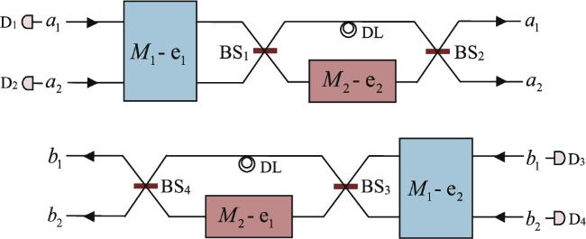
Figure 3. Schematic setup for realizing hyper-CNOT gate type II. |
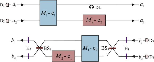
Figure 4. Schematic setup for implementing hyper-CNOT gate type III. |
After that, photon B enters the circuit from the right. In detail, photon B in both spatial modes ∣b1⟩ and ∣b2⟩ passes through the module M1-e2 and BS3. Then, photon B in ∣b2⟩ travels through the module M2-e1, and photon B in both spatial modes ∣b1⟩ and ∣b2⟩ goes through BS4. After the above processes, the state of the whole system evolves to
$\begin{eqnarray}\begin{array}{rcl}| {{\rm{\Psi }}}_{6}\rangle & = & \displaystyle \frac{1}{2}\{[{\alpha }_{1}| H{\rangle }_{A}({\gamma }_{2}| {b}_{1}\rangle +{\delta }_{2}| {b}_{2}\rangle )\\ & & +{\beta }_{1}| V{\rangle }_{A}({\gamma }_{2}| {b}_{2}\rangle +{\delta }_{2}| {b}_{1}\rangle )]| 0{\rangle }_{1}\\ & & +[{\alpha }_{1}| H{\rangle }_{A}({\gamma }_{2}| {b}_{1}\rangle +{\delta }_{2}| {b}_{2}\rangle )\\ & & -{\beta }_{1}| V{\rangle }_{A}({\gamma }_{2}| {b}_{2}\rangle +{\delta }_{2}| {b}_{1}\rangle )]| 1{\rangle }_{1}\}\\ & & \otimes \{[{\alpha }_{2}| H{\rangle }_{B}({\gamma }_{1}| {a}_{1}\rangle +{\delta }_{1}| {a}_{2}\rangle )\\ & & +{\beta }_{2}| V{\rangle }_{B}({\gamma }_{1}| {a}_{2}\rangle +{\delta }_{1}| {a}_{1}\rangle )]| 0{\rangle }_{2}\\ & & +[{\alpha }_{2}| H{\rangle }_{B}({\gamma }_{1}| {a}_{2}\rangle +{\delta }_{1}| {a}_{1}\rangle )\\ & & +{\beta }_{2}| V{\rangle }_{B}({\gamma }_{1}| {a}_{1}\rangle +{\delta }_{1}| {a}_{2}\rangle )]| 1{\rangle }_{2}\}.\end{array}\end{eqnarray}$
Finally, we measure the states of the two ancillary emitters e1 and e2 under the orthogonal basis {∣0⟩, ∣1⟩}. When the outcome is ∣0⟩1 and ∣0⟩2, the state of the two-photon system collapses to
$\begin{eqnarray}\begin{array}{rcl}| {{\rm{\Psi }}}_{7}\rangle & = & [{\alpha }_{1}| H{\rangle }_{A}({\gamma }_{2}| {b}_{1}\rangle +{\delta }_{2}| {b}_{2}\rangle )\\ & & +{\beta }_{1}| V{\rangle }_{A}({\gamma }_{2}| {b}_{2}\rangle +{\delta }_{2}| {b}_{1}\rangle )]\\ & & \otimes [{\alpha }_{2}| H{\rangle }_{B}({\gamma }_{1}| {a}_{1}\rangle +{\delta }_{1}| {a}_{2}\rangle )\\ & & +{\beta }_{2}| V{\rangle }_{B}({\gamma }_{1}| {a}_{2}\rangle +{\delta }_{1}| {a}_{1}\rangle )].\end{array}\end{eqnarray}$
We can see that the spatial-mode states of the photons B and A is simultaneously controlled by the polarization states of the photons A and B, respectively. While, if the state of the emitter e1 (e2) is ∣1⟩1 (∣1⟩2), an operation ${\sigma }_{{}^{Z}}^{{}_{P}}\,=| H\rangle \langle H| -| V\rangle \langle V| $ (${\sigma }_{{}^{X}}^{{}_{S}}=| {a}_{1}\rangle \langle {a}_{2}| +| {a}_{2}\rangle \langle {a}_{1}| $) is performed on photon A. Then, we can also obtain the state ∣$\Psi$7⟩. Therefore, the quantum circuit in figure 3 can implement the hyper-CNOT gate type II on a two-photon system.3.3. Hyper-CNOT gate type III
The schematic diagram of the hyper-CNOT gate type III is illustrated in figure 4. The polarization state and the spatial-mode state of the photon B are simultaneously controlled by the spatial-mode state and the polarization state of the photon A, respectively. The initial state of the whole system containing photons A and B and two auxiliary emitters e1 and e2 is ∣$\Psi$0⟩ given in equation (10 ), which is the same as the one of the hyper-CNOT gate type I or type II. As shown in figure 4, photon A enters the circuit from the left. In detail, photon A in spatial modes ∣a1⟩ and ∣a2⟩ goes through the module M1-e1, and then photon A in ∣a2⟩ travels through the module M2-e2. After the above processes, the state of the system is changed from ∣$\Psi$0⟩ to ∣$\Psi$8⟩, where
$\begin{eqnarray}\begin{array}{rcl}| {{\rm{\Psi }}}_{8}\rangle & = & | {{\rm{\Psi }}}_{B}\rangle \otimes ({\alpha }_{1}| H{\rangle }_{A}| 0{\rangle }_{1}+{\beta }_{1}| V{\rangle }_{A}| 1{\rangle }_{1})\\ & & \otimes ({\gamma }_{1}| {a}_{1}\rangle | 0{\rangle }_{2}+{\delta }_{1}| {a}_{2}\rangle | 1{\rangle }_{2}).\end{array}\end{eqnarray}$
After that, photon B enters the circuit from the right. First, photon B in spatial modes ∣b1⟩ and ∣b2⟩ goes through H1, BS1 and the module M1-e2. Then, photon B in ∣b2⟩ travels through the module M2-e1, and photon B in ∣b1⟩ and ∣b2⟩ goes through BS2 and H2. After that, the state of the system evolves into
$\begin{eqnarray}\begin{array}{rcl}| {{\rm{\Psi }}}_{9}\rangle & = & \displaystyle \frac{1}{2}\{[{\alpha }_{1}| H{\rangle }_{A}({\gamma }_{2}| {b}_{1}\rangle +{\delta }_{2}| {b}_{2}\rangle )\\ & & +{\beta }_{1}| V{\rangle }_{A}({\gamma }_{2}| {b}_{2}\rangle +{\delta }_{2}| {b}_{1}\rangle )]| 0{\rangle }_{1}\\ & & +[{\alpha }_{1}| H{\rangle }_{A}({\gamma }_{2}| {b}_{1}\rangle +{\delta }_{2}| {b}_{2}\rangle )\\ & & -{\beta }_{1}| V{\rangle }_{A}({\gamma }_{2}| {b}_{2}\rangle +{\delta }_{2}| {b}_{1}\rangle )]| 1{\rangle }_{1}\}\\ & & \otimes \{[{\gamma }_{1}| {a}_{1}\rangle {\left({\alpha }_{2}| H\rangle +{\beta }_{2}| V\rangle \right)}_{B}\\ & & +{\delta }_{1}| {a}_{2}\rangle {\left({\alpha }_{2}| V\rangle +{\beta }_{2}| H\rangle \right)}_{B}]| 0{\rangle }_{2}\\ & & +[{\gamma }_{1}| {a}_{1}\rangle {\left({\alpha }_{2}| H\rangle +{\beta }_{2}| V\rangle \right)}_{B}\\ & & -{\delta }_{1}| {a}_{2}\rangle {\left({\alpha }_{2}| V\rangle +{\beta }_{2}| H\rangle \right)}_{B}]| 1{\rangle }_{2}\}.\end{array}\end{eqnarray}$
Similar to type I and type II, the hyper-CNOT gate type III can be achieved by measuring the states of the two emitters e1 and e2 under the orthogonal basis {∣0⟩, ∣1⟩}. When the result is ∣0⟩1 and ∣0⟩2, the state of the two-photon system collapses into
$\begin{eqnarray}\begin{array}{rcl}| {{\rm{\Psi }}}_{10}\rangle & = & [{\alpha }_{1}| H{\rangle }_{A}({\gamma }_{2}| {b}_{1}\rangle +{\delta }_{2}| {b}_{2}\rangle )\\ & & +{\beta }_{1}| V{\rangle }_{A}({\gamma }_{2}| {b}_{2}\rangle +{\delta }_{2}| {b}_{1}\rangle )]\\ & & \otimes \{[{\gamma }_{1}| {a}_{1}\rangle {\left({\alpha }_{2}| H\rangle +{\beta }_{2}| V\rangle \right)}_{B}\\ & & +{\delta }_{1}| {a}_{2}\rangle {\left({\alpha }_{2}| V\rangle +{\beta }_{2}| H\rangle \right)}_{B}].\end{array}\end{eqnarray}$
We can find that the polarization state and the spatial-mode state of the photon A simultaneously control the spatial-mode state and the polarization state of the photon B, respectively. While, if the state of the emitter e1 (e2) is ∣1⟩1 (∣1⟩2), an operation ${\sigma }_{Z}^{P}=| H\rangle \langle H| -| V\rangle \langle V| $ (${\sigma }_{Z}^{S}=| {a}_{1}\rangle \langle {a}_{1}| -| {a}_{2}\rangle \langle {a}_{2}| $) should be performed on photon A. Then, we can also get the state ∣$\Psi$10⟩. Thus, we can realize the hyper-CNOT gate type III on a two-photon system by the the quantum circuit shown in figure 4.4. Discussion and conclusion
We have proposed some heralded schemes for constructing three types of hyper-CNOT gates in two-photon systems assisted by photon scattering in 1D waveguides. Here, the qubits are encoded in the spatial-mode and the polarization states of the photons. The basic scattering configuration shown in figure 1(b) plays a central role in our three schemes. We define its success probability as ${p}_{{}_{0}}=| \langle \psi | {\phi }_{r}\rangle {| }^{2}$, where ∣ψ⟩ and ∣φr⟩ represent the spatial wave functions of the input photon and the reflected photon part by the emitter, respectively. For a perfect scattering process, i.e., Δ = 0 and P → ∞ , we can get ∣φr⟩ = − ∣ψ⟩ and ${p}_{{}_{0}}=100 \% $. While for a realistic emitter-waveguide system, ∣φr⟩ = r∣ψ⟩ and ${p}_{{}_{0}}=| r{| }^{2}$. In this case, the faulty scattering events with unchanged photon polarization can be filtered out and discarded. Thus, our schemes for three types of hyper-CNOT gates work in a heralded way.
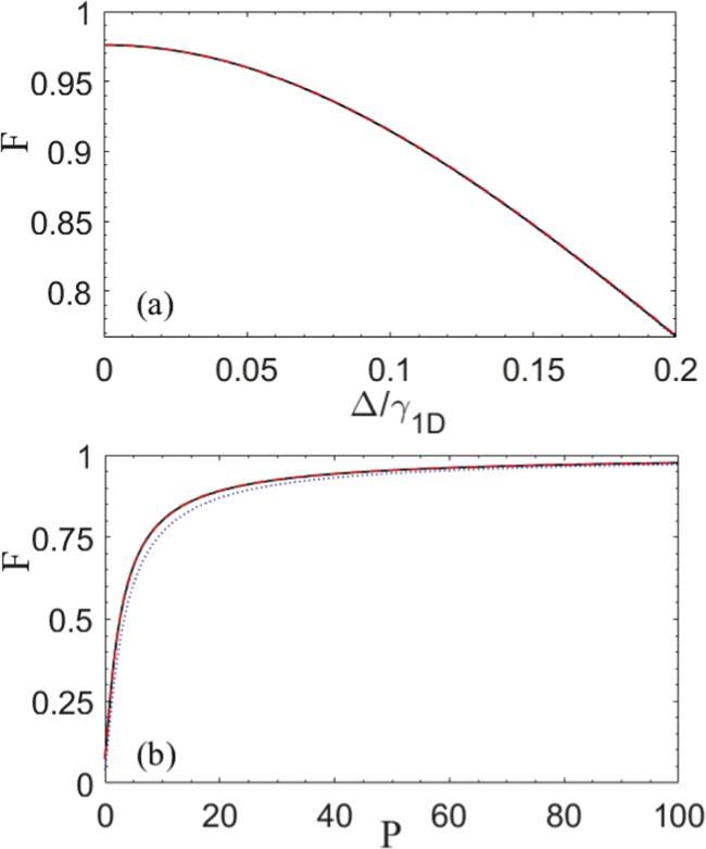
Even though our schemes work in a heralded manner, it is still important to calculate the fidelities of our three hyper-CNOT gates. The fidelity of a quantum gate is defined as F = ∣⟨Φr∣Φi⟩∣2, where ∣Φr⟩ and ∣Φi⟩ represent the final states of the two-photon system in the realistic and perfect cases, respectively. Here, the fidelities of our hyper-CNOT gates for type I, type II, and type III are marked as FI, FII, and FIII, respectively. As shown in figure 5, we present the fidelities of our three hyper-CNOT gates as a function of two important system parameters, i.e., the frequency detuning Δ and the Purcell factor P. Note that, since the fidelities of our three hyper-CNOT gates are almost the same, the three lines in figures 5 (a) or (b) coincide with each other. Figure 5(a) reveals that, the fidelities of our hyper-CNOT gates go down with the increment of the frequency detuning for a specific Purcell factor. The results in figure 5(b) show that, the fidelities of our three hyper-CNOT gates are all dramatically improved by enhancing the Purcell factor P. For example, when Δ = 0 and P = 100, the fidelities of our three gates are FI = FII = FIII = 97.6%. While, for a modest Purcell factor P = 50 with Δ = 0.05γ1D, the fidelities of the three gates become FI = 93.9%, FII = 93.8%, FIII = 93.8%, respectively. Therefore, to realize our hyper-CNOT gates with high fidelities, we should suppress the frequency detuning between the auxiliary emitters and photons, and enlarge the Purcell factor. In experiments, the four-level quantum emitter we adopt in our schemes can be realized by quantum dots. Significant progress has been reported in coupling quantum dots with waveguide systems. For example, by trapping a quantum dot in a photonic crystal waveguide, Arcari et al have obtained a high Purcell factor P ≈ 62.7 [87]. In addition, the optical transitions of a quantum dot can be frequency modulated to match the input photon by tailoring the electric fields [88].
Figure 5. The fidelities of our hyper-CNOT gates type I (black solid line), type II (red dashed line) and type III (blue dotted line) as a function of (a) the frequency detuning ${\rm{\Delta }}/{\gamma }_{{}_{1D}}$ and (b) the Purcell factor P. Parameters: (a) P = 100, (b) Δ = 0. |
The triangular scattering structure in figure 1(b) plays a crucial role in our protocols for three types of hyper-CNOT gates. Its length should be dramatically larger than the spatial size of the incident photon pulse, in which case the beam splitter can split up the photon pulse into two parts in a temporal order. In experiment, the platform for photon-emitter scattering can be obtained by interfacing single quantum dots with photonic crystal waveguides [89]. In our schemes for realizing three types of hyper-CNOT gates, faulty scattering events caused by physical imperfections, such as weak couplings, emitter's decay into undesired modes and frequency mismatches, can be transformed into the detection of photon polarization and discarded. Thus, our protocols work in a heralded manner, which is highly advantageous in quantum information applications. While, since the heralded mechanism is based on the detection of photon polarization, photon loss itself in our schemes can not be heralded. This problem can be solved by adopting specific single-photon sources, which create photons pairs via parametric down-conversion in a microstructured waveguide [90]. In such photon sources, photons are generated in pairs: one is used to encode quantum qubit, and the other is used to predict the loss of the photonic qubit. In addition, in our protocols, Hadamard operations need to be performed on the quantum emitters, which can be accomplished in picoseconds in experiment [91]. Moreover, compared with the protocols for hyperparallel quantum gates with giant Faraday rotations, our schemes based on emitter-waveguide systems have some different features. First, as we know, it is challenging for photons to go into and out of the cavities with high efficiency, which is easy for waveguide systems. Second, the emitter-waveguide system in our schemes is scalable and chip-scale integration is possible. Third, our schemes can be implemented over broadband frequencies, which is due to the continuous modes in 1D waveguides.
In summary, based on the photon scattering off single emitters in 1D waveguides, we present some heralded schemes for realizing three types of hyper-CNOT gates. The four qubits of our hyper-CNOT gates are encoded on both the polarization and spatial-mode DOFs of the photons, which expands the quantum channel capacity, reduces the photonic dissipation noise, and improves the computation speed. Moreover, faulty scattering events in our protocols can be filtered out and discarded, which is an advantageous feature for quantum computation and quantum information processing. That is, our schemes work in a heralded manner. The recent significant progress in emitter-waveguide systems implies that our hyper-CNOT gates may be feasible with high fidelities.