


1. Introduction
Thermal stress, growth stress and interface stress collectively constitute the residual stress, which is mainly caused by grain growth behavior, lattice mismatch or chemical reaction [1–3]. Many works have studied the effects of different parameters in growth stress and interface stress [4, 5]. Reports on thermal stress are usually not specific enough, but it is common in multilayer film-substrate systems [6–8]. Thermal stress is affected by the coefficient of thermal expansion (CTE), Young's modulus, thermal conductivity [9, 10] and other parameters. Notably, when there is a significant difference in the CTEs of the materials, leading to a mismatch between layers, the contribution of thermal stress to the overall residual stress becomes substantial [11–14].
Han et al established a physical model to study the causes of cracks in films during laser ablation, concluding that thermal stress plays a significant role [15]. Using finite element analysis, Ranade et al simulated stress distribution to understand the impact of strain on the generation and propagation of coating defects, analyzing defect paths [16]. Li et al measured the thermal stress of the structure based on the Raman peak method, and combined with the simulation, improved the accuracy of the conclusion [17]. However, these studies primarily focused on the distribution or sources of thermal stress within structures [18–21], and few works discussed how to weaken or eliminate thermal stress in the system. Mori et al reduced the influence of thermal stress by changing the film material [22], while Travis et al explored the relationship between thermal expansion mismatch and film thickness, reducing thermal stress by adding an additional film layer to the substrate [23]. These studies discuss how to reduce thermal stress, but mostly revolve around changing the design of the substrate or film or focusing on the influence of the fabrication process and deposition temperature [24–26]. To specifically address how to reduce the thermal stress mutation without changing the general film design, we employed chamfering and introduced an intermediate layer. The results indicate that a larger chamfer significantly reduces thermal stress concentration, and that a smaller CTE and a harder primer layer further diminish stress mutations within the inner layer.
In this paper, we simulated a multilayer structure to calculate the thermal stress generated when the ambient temperature increases from 20 °C to 80 °C. Due to the right angle at the base of the structure's side, a sudden concentration of thermal stress occurs. The significant difference in CTEs between the different materials leads to a substantial thermal stress discontinuity between the film layers. To address this, we investigated the effects of chamfering and adding an intermediate layer, which significantly weakened the thermal stress concentration and reduced the thermal stress differences. This study provides a new solution for reducing thermal stress concentration points and stress discontinuities.
2. Modeling and simulation
2.1. Assumption
The modeling in this paper is based on the following assumptions:
| (1)the materials are all linear elastic and isotropic, | |
| (2)the film and the substrate are perfectly bonded at the boundary, | |
| (3)the structure is in a stable temperature field environment, | |
| (4)no initial residual stress, | |
| (5)the temperature dependence of CTE is negligible. |
2.2. Establishment of a structural model
In this paper, based on COMSOL Multiphysics software for modeling and simulation, the thermal stress distribution in a multilayer film system is calculated and analyzed [27–29]. We established key boundary conditions, including setting rigid motion suppression to prevent rigid displacement and rotation, ensuring model stability, simulating real boundary conditions, and setting the temperature to simulate changes in the ambient temperature. The multilayer structure we constructed is shown in figure 1(b). The substrate is disc-shaped polystyrene (PS), on which Ag, NiCr and Si3N4 are successively deposited. These coatings, typically obtained through plasma spraying, have a wide range of applications. For example, in microelectronic devices, Ag can be used as a conductive coating, NiCr as a resistance material and Si3N4 as a protective layer to prevent wear and corrosion. Considering the symmetry of the structure and the amount of calculation of the 3D structure, we used a 2D axisymmetric model, as shown in figure 1(a), and used rotation to obtain the calculation results under the 3D structure. The thickness of the substrate PS layer H1 = 3000 nm, and the radius R1 = 4500 nm. The thicknesses of the Ag, NiCr and Si3N4 films are 300, 100 and 100 nm, respectively. The rationale for selecting these dimensions is explained in figure S1. The physical parameters of each material are shown in table 1, and the meanings of each symbol are organized in table 2.
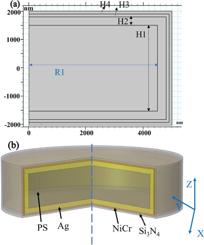
Figure 1. (a) 2D axisymmetric diagram of the structure; (b) 3D view of the structure. |
Table 1. Mechanical and thermal parameters of each material. |
| Materials | Young's modulus (Pa) | Poisson's ratio | Density (kg m−3) | Thermal expansion coefficient (1/K) |
|---|---|---|---|---|
| PS | 3.3 × 10⁹ | 0.32 | 1120 | 8.0 × 10⁻⁵ |
| Ag | 7.3 × 10¹⁰ | 0.38 | 10490 | 1.9 × 10⁻⁵ |
| NiCr | 2.0 × 10¹¹ | 0.29 | 8200 | 1.3 × 10⁻⁴ |
| Si3N4 | 3.7 × 10¹¹ | 0.25 | 3100 | 3.0 × 10⁻⁶ |
Table 2. List of symbols. |
| Symbol | Description | Unit |
|---|---|---|
| α | Coefficient of thermal expansion | 1/K |
| αf | Coefficient of thermal expansion of film | Pa |
| αs | Coefficient of thermal expansion of substrate | Pa |
| γ | Shear strain on the plane | — |
| ϵ | Stress on the plane | Pa |
| σ | Strain on the plane | — |
| &ugr; | Poisson's ratio | — |
| &ugr;f | Poisson's ratio of film | — |
| &ugr;s | Poisson's ratio of substrate | — |
| τ | Shear stress on the plane | Pa |
| E | Young's modulus | Pa |
| Ef | Young's modulus of film | Pa |
| Es | Young's modulus of substrate | Pa |
| Fx | Components of the unit volume force on the x axis | N |
| Fy | Components of the unit volume force on the y axis | N |
| Fz | Components of the unit volume force on the z axis | N |
| G | Shear modulus | — |
| h | Thickness of film | nm |
| H | Thickness of substrate | nm |
| T | Temperature | K |
| Tr | Room temperature | K |
| Td | Ambient temperature | K |
3. Thermal stress analysis in multilayers
3.1. Mathematical model of thermodynamic analysis
Constitutive equation:
$\begin{eqnarray}{\varepsilon }_{x}=\displaystyle \frac{1}{E}\left\{{\sigma }_{x}-\nu \left({\sigma }_{y}+{\sigma }_{z}\right)\right\}+\alpha T,{\tau }_{yz}=G{\gamma }_{\rm{yz\unicode{x000A0}}},\end{eqnarray}$
$\begin{eqnarray}{\varepsilon }_{{\rm{y}}}=\displaystyle \frac{1}{E}\left\{{\sigma }_{{\rm{y}}}-\nu \left({\sigma }_{z}+{\sigma }_{x}\right)\right\}+\alpha T,{\tau }_{zx}=G{\gamma }_{zx},\end{eqnarray}$
$\begin{eqnarray}{\varepsilon }_{{\rm{z}}}=\displaystyle \frac{1}{E}\left\{{\sigma }_{{\rm{z}}}-\nu \left({\sigma }_{x}+{\sigma }_{y}\right)\right\}+\alpha T,{\tau }_{\rm{xy}}=G{\gamma }_{xy}.\end{eqnarray}$
The equilibrium differential equation of equation (1a ) is:
$\begin{eqnarray}\displaystyle \frac{\partial {\sigma }_{x}}{\partial x}+\displaystyle \frac{\partial {\tau }_{yx}}{\partial y}+\displaystyle \frac{\partial {\tau }_{zx}}{\partial z}+Fx=0,\end{eqnarray}$
$\begin{eqnarray}\displaystyle \frac{\partial {\tau }_{xy}}{\partial x}+\displaystyle \frac{\partial {\sigma }_{y}}{\partial y}+\displaystyle \frac{\partial {\tau }_{\mathrm{yz}}}{\partial z}+Fy=0,\end{eqnarray}$
$\begin{eqnarray}\displaystyle \frac{\partial {\tau }_{\mathrm{xz}}}{\partial x}+\displaystyle \frac{\partial {\tau }_{\mathrm{yz}}}{\partial z}+\displaystyle \frac{\partial {\sigma }_{z}}{\partial {\rm{z}}}+Fz=0.\end{eqnarray}$
Strain displacement equation [32, 33]:
$\begin{eqnarray}{\varepsilon }_{x}=\displaystyle \frac{\partial u}{\partial x},{\varepsilon }_{{\rm{y}}}=\displaystyle \frac{\partial \nu }{\partial y},{\varepsilon }_{z}=\displaystyle \frac{\partial w}{\partial z},\end{eqnarray}$
$\begin{eqnarray}{\gamma }_{\rm{yz}}=\displaystyle \frac{\partial \nu }{\partial y}+\displaystyle \frac{\partial w}{\partial z},{\gamma }_{zx}=\displaystyle \frac{\partial u}{\partial x}+\displaystyle \frac{\partial w}{\partial z},{\gamma }_{xy}=\displaystyle \frac{\partial u}{\partial x}+\displaystyle \frac{\partial \nu }{\partial y}.\end{eqnarray}$
Finally, the shear modulus is obtained:
$\begin{eqnarray}{G}_{\mathrm{sm}}=\displaystyle \frac{E}{2\left(1+\nu \right)}.\end{eqnarray}$
In this study, to provide a specific value for thermal stress, we use the first principal stress of von Mises stress for evaluation and analysis. Von Mises stress is an equivalent stress based on shear strain energy, taking into account the first, second and third principal stresses. It can be used to evaluate fatigue, failure and other factors. In addition, it uses the stress contour to represent the stress distribution inside the model, which can clearly describe the change of a result in the whole model [34].
The von Mises equivalent stress is expressed as [35, 36]:
$\begin{eqnarray}{\sigma }_{\mathrm{eq}}=\sqrt{\displaystyle \frac{1}{2}\left[{\left({\sigma }_{x}-{\sigma }_{y}\right)}^{2}+{\left({\sigma }_{y}-{\sigma }_{z}\right)}^{2}+{\left({\sigma }_{z}-{\sigma }_{x}\right)}^{2}+6{\tau }_{\rm{xy}}^{2}+{\tau }_{yz}^{2}+{\tau }_{\rm{zx}}^{2}\right]}.\end{eqnarray}$
3.2. Thermal stress analysis in multilayer structure
The boundary temperature of the multilayer system increases from room temperature 20 °C (293.15 K) to 80 °C (353.15 K) at a rate of 6 °C min−1. To observe the thermal stress between the layers of each film more conveniently and intuitively, as shown in figure 2(a), we selected a red cross-section that runs through the multilayer to study the thermal stress distribution at different locations.
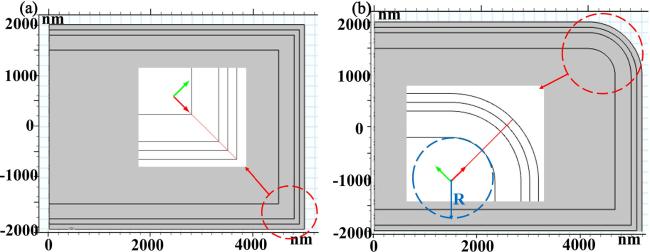
Figure 2. (a) Selection method for 2D cutting lines with right angles; (b) selection method for 2D cutting lines with rounded corners. |
In figure 3(a), the thermal stress between the corresponding layers is given. With the increase in temperature in the multilayer film system, the thermal stress value of each film layer increases, up to 4.79 × 10⁸ N m−2 (as marked in figure 3(b)), and the extrusion between layers is more serious, causing an increase in the thermal stress difference between the corresponding film layers [15, 32], such as the thermal stress difference between the PS and Ag layers that increased to 4.38 × 10⁸ N m−2. In addition, the stress mutation between the PS and Ag layers, as well as between the NiCr and Si3N4 layers, becomes more pronounced. According to table 1, the CTE of PS is 8 × 10⁻⁵ 1/K, while that of Ag is 1.9 × 10⁻⁵ 1/K, reflecting an order-of-magnitude difference. There is also a large gap in the CTE between the NiCr and Si3N4 layers. The extreme mismatch of the CTE results in a large extrusion between the layers and a significant thermal stress difference. Notably, a thermal stress concentration point occurs at the corner between the PS and Ag layers, reaching 3.31 × 10⁸ N m−2, which increases the risk of crack propagation and film delamination [37]. To solve the stress mutation and thermal stress concentration point between the substrate and the film layer, we subsequently studied methods to reduce or eliminate these issues.
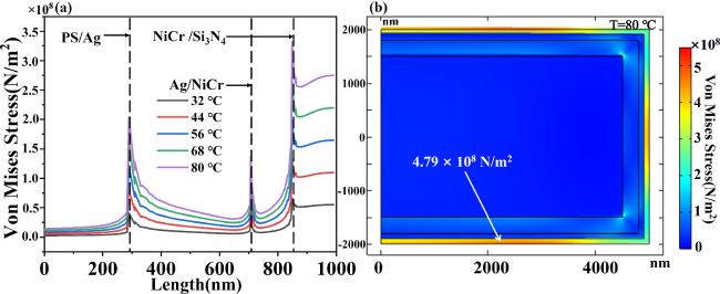
Figure 3. (a) Thermal stress value from 32 °C to 80 °C obtained at the 2D cut line; (b) thermal stress distribution at the structural temperature of 80 °C. |
To illustrate the compression and deformation caused by the thermal stress between layers, we present the relationship between thermal stress and deformation at different temperatures. Figure 4 highlights the situation at the corners of the structure. At 32 °C, the thermal stress variation in the multilayer system is not pronounced, although there is some thermal stress disparity between the PS and Ag layers [38]. As the temperature rises to 56 °C, the thermal stress variation between the layers becomes more evident, and a slight thermal stress concentration begins to emerge between the Ag and NiCr layers [39]. To explain the changes in thermal stress caused by temperature change, we can define the thermal stress equation in the film by the Stoney equation [40]:
$\begin{eqnarray}\sigma =\displaystyle \frac{{E}_{{\rm{e}}{\rm{f}}}{\int }_{{T}_{r}}^{{T}_{d}}\left({a}_{s}-{a}_{f}\right){\rm{d}}T}{1+4\left(\tfrac{{E}_{\mathrm{ef}}}{{E}_{\mathrm{es}}}\right)\left(\tfrac{h}{H}\right)}.\end{eqnarray}$
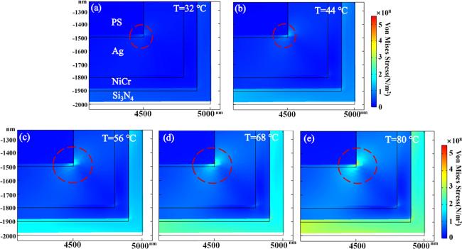
Figure 4. (a)–(e) Thermal stress between and in the film when the structure temperature increases from 32 °C to 80 °C. |
Among them, the CTE has a significant impact. According to the thermal stress equation, as the temperature increases, the expansion of materials with different CTEs is different, materials with different CTEs expand at different rates, leading to increased disparity in expansion between layers and greater compression, which causes a sudden rise in thermal stress [41]. As the temperature continues to rise, the thermal stress difference between the layers of each film continues to grow. The stress differences are 43.8 × 10⁷ N m−2 between the PS and Ag layers, 3.91 × 10⁷ N m−2 between the Ag and NiCr layers and 33.91 × 10⁷ N m−2 between the NiCr and Si3N4 layers. At T = 80 °C, the thermal stress difference reaches 47.9 × 10⁷ N m−2, with the maximum stress occurring at the corners of the PS layer. The large magnitude of thermal stress difference and concentration makes the film prone to delamination, which is detrimental in practical applications.
Young's modulus and Poisson's ratio also affect thermal stress. However, the materials in this paper have similar Poisson's ratios, resulting in a weak influence. There is a significant difference in Young's modulus between the PS layer (3.3 × 10⁹ Pa) and the Ag layer (7.3 × 10¹⁰ Pa), as well as between other film layers. According to equation (6 ), the difference in Young's modulus is another factor contributing to the sudden change in stress between the film layers.
4. Reducing the thermal stress mismatch in multilayers
4.1. The influence of chamfering on the thermal stress concentration point
According to previous research, the thermal stress concentration point is located at the edge of the multilayer film system. To address this, we applied chamfering to release the thermal stress discontinuities, resulting in a smoother thermal stress transition [42]. As shown in figure 2(b), the red dotted line illustrates our chamfering approach. To smooth the edge transition at the chamfer, we set the chamfer to a concentric fillet, and the fillet radius of the PS layer is expressed as R. The 2D section line was selected along the diagonal, consistent with the earlier method.
Figures 5(a)–(c) show the thermal stress distribution for three different chamfer radii R (1000, 1500, 2000 nm). As shown, for the first stress mutation position between the PS and Ag layers, the stress difference under the three chamfering radii is below 5 × 10⁷N m−2. Compared to the initial stress difference of 43.8 × 10⁷ N m−2, the stress discontinuity has been greatly alleviated. When R = 1000 nm, the thermal stress difference between the PS and Ag layers is 2.73 × 10⁷ N m−2, and when R = 2000 nm, the difference is 2.36 × 10⁷ N m−2. As shown in figure 6, as R increases, the thermal stress concentration point between the PS and Ag layers gradually decreases until it nearly disappears. Figure 5(d) shows that for the second stress mutation point, between the Ag and NiCr layers, when R increases from 1000 to 2000 nm, the corresponding black curve gently transitions to the blue curve. To show the relationship more intuitively between thermal stress difference and chamfer radius R, we provided thermal stress values for different radius values. Table 3 shows that the stress difference between the Ag and NiCr layers decreases from 0.99 × 10⁷ N m−2 to -0.07 × 10⁷ N m−2, indicating a shift from expansion to slight compression. It is worth noting that the stress difference between the NiCr and Si3N4 layers in figure 5(d) appears almost unaffected by the radius. However, numerical calculations show a decrease from 3.148 × 10⁸ N m−2 to 2.982 × 10⁸ N m−2.
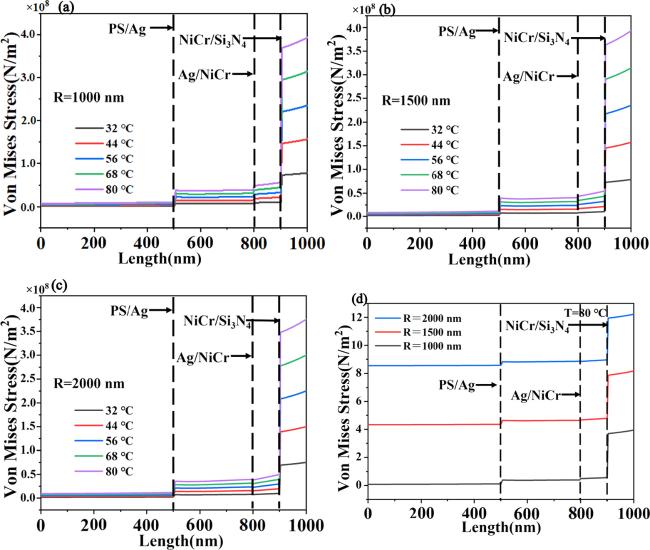
Figure 5. (a)–(c) When the chamfer radius is 1000, 1500 and 2000 nm, respectively, the thermal stress value with the temperature rises from 32 °C to 80 °C. (d) When the temperature is 80 °C, the thermal stress at three chamfer radii are compared. |
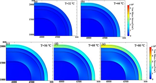
Figure 6. When temperature is at 80 °C, the thermal stress diagrams of three different chamfer radii. |
Table 3. When the temperature is 80 °C, the thermal stress difference between the film layers under three chamfer radii. |
| Chamfer radius | Thermal stress difference of PS-Ag (N m−2) | Thermal stress difference of Ag-NiCr (N m−2) | Thermal stress difference of NiCr-Si3N4 (N m−2) |
|---|---|---|---|
| 1000 nm | 2.73 × 10⁷ | 0.99 × 10⁷ | 31.48 × 10⁷ |
| 1500 nm | 2.73 × 10⁷ | 0.32 × 10⁷ | 30.87 × 10⁷ |
| 2000 nm | 2.36 × 10⁷ | -0.07 × 10⁷ | 29.82 × 10⁷ |
Based on previous research, for mitigating the sudden change in thermal stress in the multilayer film system, the larger the chamfer radius R, the more effective it is at reducing stress concentration points and discontinuities.
Observing the stress between the PS and Ag layers in figures 6(a)–(c), it is found that the stress discontinuity gradually decreases and becomes almost unnoticeable when the chamfer radius reaches 2000 nm. A similar trend is observed for the stress discontinuity between the Ag and NiCr layers. Through numerical calculation, the stress difference between the NiCr and Si3N4 layers decreases from 31.48 × 10⁷ N m−2 to 29.82 × 10⁷ N m−2. This indicates that a larger chamfer radius reduces the geometric section size, making the release of stress concentration more effective.
4.2. The effect of increasing the intermediate layer on the sudden change of thermal stress
We also added an intermediate layer directly without chamfering. Figure 7 shows the variation of thermal stress with temperature and arc length at the 2D section, and figure 8 shows the local thermal stress. In figures 7 and 8, (a) shows the addition of acrylic resin, (b) shows the addition of fluorocarbon, (c) shows the addition of epoxy polyamide and (d) shows the addition of epoxy resin. Compared to adding an intermediate layer based on chamfering, directly adding the intermediate layer shows similar results. Although the addition of fluorocarbon reduces the thermal stress concentration point, it increases the thermal stress difference between the remaining film layers. In figure 8(b), the thermal stress of the entire Si3N4 film even reaches its maximum value, and a new thermal stress concentration point also appears at the corners of the Ag and NiCr layers [43]. The other three intermediate layers, with smaller thermal expansion coefficients, are more effective at reducing both thermal stress differences and concentration points.
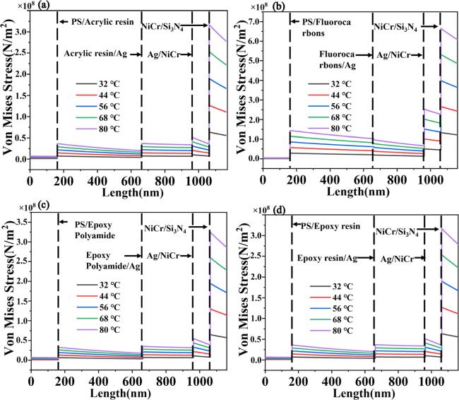
Figure 7. Different intermediate layer added between the PS and Ag layers without chamfering. Added intermediate layers are (a) acrylic resin; (b) fluorocarbons; (c) epoxy polyamide; (d) epoxy resin. |
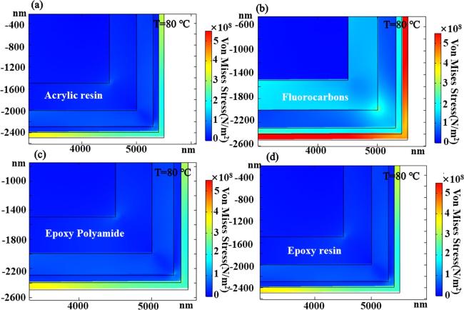
Figure 8. Thermal stress diagrams at 80 °C with different intermediate layers. |
In addition to using chamfering to alleviate thermal stress concentration, the mismatch between film layers due to differing CTEs and other parameters must also be considered [44]. Therefore, to address the thermal stress concentration (with a chamfering radius R = 2000 nm), we selected several types of intermediate layers and provided their mechanical and thermal parameters, as shown in table 4.
Table 4. Mechanical and thermal parameters of different intermediate layers. |
| Materials | Young's modulus (Pa) | Poisson's specific | Density (kg m−3) | Thermal expansion coefficient (1/K) |
|---|---|---|---|---|
| Acrylic resin | 1.00 × 10¹⁰ | 0.17 | 1090 | 1.00 × 10⁻⁶ |
| Fluorocarbons | 6.60 × 10¹⁰ | 0.17 | 1280 | 5.76 × 10⁻⁵ |
| Epoxy polyamide | 1.00 × 10¹⁰ | 0.17 | 1300 | 6.00 × 10⁻⁶ |
| Epoxy resin | 1.00 × 10¹⁰ | 0.193 | 1300 | 1.00 × 10⁻⁶ |
Considering the large difference in thermal stress between the PS and Ag layers, we used paint as an intermediate layer (thickness: 500 nm) and studied the resulting thermal stress, as shown in figure 10. By observing and comparing figures 9(a)–(d) and 10(a)–(d), the thermal stress concentration points between the PS and Ag layers are almost greatly reduced, indicating that the addition of certain primers can effectively reduce thermal stress concentration points. However, the addition of fluorocarbon has a less favorable effect on reducing the thermal stress concentration point and leads to increased stress discontinuities between the remaining film layers [45]. As shown in figures 9(b) and 10(b), after adding fluorocarbon, the stress difference between the Ag and NiCr layers and between the NiCr and Si3N4 layers is significantly higher than with other intermediate layers, reaching 18.64 ×10⁷ N m−2 and 43.93 × 10⁷ N m−2, even far exceeding the stress difference without chamfering and adding an intermediate layer: 3.91 × 10⁷ N m−2 and 33.91 × 10⁷ N m−2. The other three intermediate layers show similar effects in reducing stress discontinuities, significantly weakening stress mutations between the film layers.
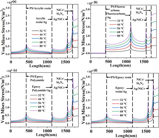
Figure 9. (a)–(d) After adding different intermediate layers, the thermal stress changes with the increase in temperature. |
Figure 10. Intermediate layer added while the chamfer radius is 2000 nm. |
Theoretically, the CTE of fluorocarbon is 5.76 × 10⁻⁵ 1/K. In the PS and Ag layers, the CTE mismatch between the layers should be reduced after adding fluorocarbon, resulting in a reduction of stress differences between the film layers [14], and this reduction effect should be better than with the other three materials. However, the conclusion of this study differs from the theoretical expectation, primarily due to the influence of Young's modulus [46]. As shown in table 3, the Young‘s modulus of fluorocarbon is 6.6 × 10¹⁰ Pa, which is much higher than the 1.0 × 10¹⁰ Pa of the other intermediate layer coatings. The greater hardness of fluorocarbon results in a weaker reduction of thermal stress concentration points [47]. Due to its larger Young‘s modulus, the stress between the remaining film layers increases abruptly [48]. Subsequently, in table 5, we confirmed this finding by numerical calculation. The addition of fluorocarbon reduces the thermal stress difference between the Ag and NiCr layers to -0.63 × 10⁷ N m−2, while the thermal stress differences between the remaining layers are 9.71 × 10⁷ N m−2,18.64 × 107 N m−2 and 43.93 × 10⁷ N m−2, respectively, which is significantly larger than with other primers, such as acrylic resin as the intermediate layer. For acrylic resin, the thermal stress differences between the corresponding layers are 3.02 × 10⁷ N m−2, 1.68 × 10⁷ N m−2 and 28.15 × 10⁷ N m−2. The weakening effect of the other primers on the thermal stress concentration point and the stress difference is similar [49]. Therefore, the selected primer should have both a lower CTE and a lower Young's modulus; that is, a primer with lower hardness can more effectively mitigate stress discontinuities [50].
Table 5. The thermal stress difference between the film layers when different intermediate layers are added, respectively. |
| Intermediate layer | Thermal stress difference of PS intermediate layer (N m−2) | Thermal stress difference of intermediate layer Ag (N m−2) | Thermal stress difference of Ag NiCr (N m−2) | Thermal stress difference of NiCr Si3N4 (N m−2) |
|---|---|---|---|---|
| Acrylic resin | 3.02 × 10⁷ | 1.68 × 10⁷ | 1.74 × 10⁷ | 28.15 × 10⁷ |
| Fluorocarbons | 9.71 × 10⁷ | −0.63 × 10⁷ | 18.64 × 10⁷ | 43.93 × 10⁷ |
| Epoxy polyamide | 2.65 × 10⁷ | 1.75 × 10⁷ | 2.32 × 10⁷ | 28.61 × 10⁷ |
| Epoxy resin | 3.00 × 10⁷ | 1.69 × 10⁷ | 1.75 × 10⁷ | 28.15 × 10⁷ |
5. Conclusion
In this paper, the internal thermal stress of a multilayer film system is simulated and calculated. It is found that there is a significant stress discontinuity between the film layers, with a pronounced thermal stress concentration point at the corner of the PS substrate and the Ag film, where the thermal stress reaches its maximum value of 4.79 × 10⁸ N m−2. The larger stress difference and thermal stress concentration point make the multi-film system prone to cracking and delamination. To address the primary thermal stress concentration, we achieved better results by chamfering the concentric circles at R = 2000 nm. Building on this and considering the mismatch between film layers due to different parameters, such as the CTE of the materials, we added an intermediate layer between the PS and Ag layers. The results show that a primer with a lower CTE and a lower Young's modulus is more effective in reducing thermal stress concentration points and stress discontinuities. Unlike other studies that focus solely on thermal stress distribution or material selection for the substrate and film, we use chamfering and the addition of an intermediate layer between the film layers to address thermal stress concentration points. This approach has yielded superior results and provides a valuable reference for related research.