


1. Introduction
Metamaterials have become a hot topic in research into wave-absorbing materials in recent years due to their perfect wave-absorbing properties, but conventional metamaterial absorbers are passive wave absorbers that have the disadvantage that their wave-absorbing properties cannot be changed once they are prepared and moulded. Therefore, tunable metamaterial absorbers have gradually become one of the main directions of research in various fields [1, 2]. Tunable materials are materials that can change their electromagnetic properties according to external excitation; common external excitations include externally applied voltage, laser light, etc. The external excitation changes the conductivity or dielectric constant and other electromagnetic parameters of the tunable material, while at the same time its topology does not change. These excellent characteristics of tunable materials make them particularly useful [3]. Common tunable materials include graphene, vanadium dioxide (VO2), photosensitive silicon and, especially, graphene, which has been a focus of research in the field of absorbers in recent years [4–6]. Graphene is a nanomaterial in which carbon atoms connected by sp2 hybridisation are tightly packed into a single two-dimensional honeycomb lattice structure. The standard thickness of a single layer of graphene is only $0.334\,{\rm{nm}},$ with the thickest layer not exceeding $0.4\,{\rm{nm}}.$ Graphene’s unique physical structure gives it excellent optical, electrical and mechanical properties, and because the structure is a single layer of carbon atoms, graphene has superior electrical conductivity [7, 8]. Although graphene has many excellent properties, it also has some disadvantages. For example, the inability to exist stably in an aerobic environment is a huge disadvantage of graphene: if it reacts with oxygen at high temperatures this will lead to the generation of graphene oxide, resulting in the destruction of its properties until it loses its conductive properties. Dirac semimetals have also attracted attention for their excellent optical properties [9–11] and were found to have a linear dispersion relation very similar to that of graphene. The electrons in them behave as zero-mass fermions, yielding unique optical, magnetic and transport properties, and they are therefore considered to be three-dimensional analogues of graphene. Dirac semimetallic films have the advantages of photosensitive two-dimensional materials and are less susceptible to dielectric interference; unlike graphene they have no excess surface electrons [12, 13]. In addition, the carrier mobility in Dirac semimetal films can reach $9\times {10}^{6}\,{\mathrm{cm}}^{2}\,{{\rm{V}}}^{-1}\,{{\rm{s}}}^{-1},$ which is much higher than the best value for graphene. Remarkably, their conductivity can be dynamically altered by alkaline surface doping by changing the Fermi energy level. These properties ensure that the use of Dirac semimetallic materials for the design of terahertz absorbers has a variety of significant advantages, such as: flexible tunability and stable controllability, efficient terahertz absorption and wider bandwidth response [14, 15]. These advantages of Dirac semimetals mean that they are increasingly being used in terahertz imaging and detection, terahertz communication systems, high-performance optoelectronic devices and other fields. Dirac semimetallic materials are of various types—topological Dirac semimetallic, three-dimensional Dirac semimetallic and two-dimensional Dirac semimetallic—and it is the topological Dirac semimetal Na3Bi that is considered in this paper.
VO2 is a new type of phase change material with metal–insulator transition and structural phase change properties that changes its own structural state when the external environment changes. For example, VO2 can change from an insulator to a metallic state when stimulated by electricity, heat and light. Alterations to the structural state of VO2 can change its conductivity by four to five orders of magnitude. Up to now, VO2 has been integrated into terahertz metamaterials and has realised a variety of active functions, such as transmission control, phase modulation, tunable absorbers and switchable multifunctional devices. Due to the unique physical properties of Dirac semimetals and VO2, the use of Dirac semimetals and VO2 in the design of dual-tuned metamaterial absorbers has become a popular research topic [16, 17]. For example, Hu et al proposed a dynamic dual-tuned multi-band absorber based on a Dirac semimetal and VO2 [18] and Meng et al proposed a terahertz coherent dual-tuned absorber based on VO2 and a Dirac semimetal [19].
In this paper, a three-layer tunable absorber based on a Dirac semimetal is designed and the effect of changing the relevant structural parameters on the performance of the absorber is analysed. The substructure is then fabricated from VO2 polycrystals based on their material properties. Finally, the tunability of the conductivity of the Dirac semimetal is exploited to achieve dynamic tuning of the absorption frequency by varying the Fermi energy levels of the Dirac semimetal without the need to optimise the geometry and refabricate the structure.
2. Dirac semimetal properties
The electrical conductivity σ of Dirac semimetals is affected by factors such as the Fermi level EF, frequency ω, ambient temperature T, etc. According to the Kubo formula, the electrical conductivity of a Dirac semimetallic material can be expressed as [20]
$\begin{eqnarray}{\sigma }_{\mathrm{intra}}=\displaystyle \frac{{\rm{i}}{e}^{2}}{\hslash }\displaystyle \frac{g{k}_{{\rm{F}}}}{{{6}{\pi }}^{2}{\rm{\Omega }}}\left(1+\displaystyle \frac{{\pi }^{2}}{3}{\left(\displaystyle \frac{T}{{E}_{{\rm{F}}}}\right)}^{2}\right)\,\end{eqnarray}$
$\begin{eqnarray}\begin{array}{l}{\sigma }_{\mathrm{inter}}=\displaystyle \frac{{\rm{i}}{e}^{2}gw}{3{\pi }^{2}\hslash {\upsilon }_{{\rm{F}}}}\left[-\displaystyle \frac{\pi {\rm{i}}}{2}\displaystyle \frac{G\left(\tfrac{\hslash \omega }{2}\right)}{4}\right.\\ \,\left.+\,{\int }_{0}^{\infty }\displaystyle \frac{G\left(E\right)-G\left(h\omega /2\right)}{{h}^{2}{\omega }^{2}-4{E}^{2}}E{\rm{d}}E\right]\,\end{array}\end{eqnarray}$
where ${\sigma }_{\mathrm{intra}}$ is the intra-band conductivity, ${\sigma }_{{\rm{inter}}}$ is the inter-band conductivity, G is the degeneracy factor [21], ${k}_{{\rm{F}}}={E}_{{\rm{F}}}/\hslash {\upsilon }_{{\rm{F}}}$ is the Fermi momentum, ${V}_{{\rm{F}}}=c/300$ is the Fermi velocity and ${E}_{{\rm{F}}}$ is the Fermi level. According to the stochastic phase approximation theory, the real and imaginary parts of the conductivity of Dirac semimetallic materials can be expressed as $\begin{eqnarray}{\mathrm{Re}}_{{\rm{\sigma }}}\left({\rm{\Omega }}\right)=\displaystyle \frac{{e}^{2}g{k}_{{\rm{F}}}}{24\pi \hslash }{\rm{\Omega }}G\left({\rm{\Omega }}/2\right),\end{eqnarray}$
$\begin{eqnarray}{\mathrm{Im}}_{\sigma }\left({\rm{\Omega }}\right)=\displaystyle \frac{{e}^{2}g{k}_{{\rm{F}}}}{24{\pi }^{2}\hslash }\left[\displaystyle \frac{4}{{\rm{\Omega }}}-{\rm{\Omega }}\,\mathrm{ln}\left(\displaystyle \frac{{4\varepsilon }_{{\rm{c}}}^{2}}{\left|{\Omega }^{2}-4\right|}\right)\right],\end{eqnarray}$
where ${\rm{\Omega }}=\hslash \omega {/E}_{{\rm{F}}}+{\rm{i}}\hslash {\tau }^{-1}{/E}_{{\rm{F}}},\tau {=\mu E}_{{\rm{F}}}/e{\upsilon }^{2}F$ is the relaxation time, $\mu $ is the carrier mobility, ${\varepsilon }_{{\rm{c}}}={E}_{{\rm{C}}}/{E}_{{\rm{F}}}$ (${E}_{{\rm{C}}}$ is the cut-off energy of the non-linear spectral spectrum of the Dirac material). When the conductivity of the Dirac semimetallic material is obtained, its effective permittivity can be expressed as $\begin{eqnarray}\begin{array}{l}\varepsilon \left({\rm{\Omega }}\right)={\varepsilon }_{{\rm{b}}}+{\rm{i}}\left\{\displaystyle \frac{{e}^{2}g{k}_{{\rm{F}}}}{24\pi \hslash }{\rm{\Omega }}G\left({\rm{\Omega }}-2\right)\right.\\ \,\left.+\,{\rm{i}}\displaystyle \frac{{e}^{2}g{k}_{{\rm{F}}}}{24\pi \hslash }\left[\displaystyle \frac{4}{{\rm{\Omega }}}-{\rm{\Omega }}\,\mathrm{ln}\left(\displaystyle \frac{4{\varepsilon }_{{\rm{c}}}^{2}}{{\Omega }^{2}-4}\right)\right]\right\}/{\varepsilon }_{0}\omega .\end{array}\end{eqnarray}$
Based on the above equations, the normalised conductivity and dielectric constant of the Dirac semimetallic material can be obtained. Figure 1 shows the conductivity and dielectric constant of a Dirac semimetallic material at a energy level of $10\,{\rm{meV}}$.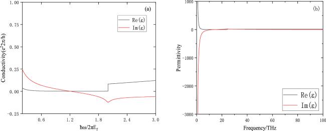
Figure 1. Dirac semimetal with (a) conductivity and (b) dielectric constant at a Fermi energy level of 10 meV. |
3. Structure and working principle of the absorber
The structure of the novel tunable absorber based on a Dirac semimetal proposed in this section is shown in figure 2. The absorber consists of three different layers with a cell period of $p=13.5\,{\rm{\mu }}{\rm{m}}$: these are, from top to bottom, a double semicircular Dirac semimetal resonator, a silicon dioxide (SiO2) substrate and a continuous VO2 reflector. The two semicircular resonators have an outer-ring radius ${R}_{2}\,=\,3.5\,{\rm{\mu }}{\rm{m}}$ and an inner-ring radius ${R}_{1}\,=\,0.875\,{\rm{\mu }}{\rm{m}}$; the width of the ring $\omega \,=\,0.8\,{\rm{\mu }}{\rm{m}}.$ The heights of the top Dirac semimetallic layer, the intermediate SiO2 dielectric layer and the bottom VO2 layer are respectively ${h}_{1}\,=\,1.25\,{\rm{\mu }}{\rm{m}},$ ${h}_{2}=0.2\,{\rm{\mu }}{\rm{m}}$ and ${h}_{3}=0.325\,{\rm{\mu }}{\rm{m}},$ and the refractive index of silica is taken as 1.97. The structural parameters are given in table 1. The model is designed in CST MWS software (version 2022) by allowing the electromagnetic waves to be incident vertically along the negative direction of the Z-axis and the electric field to be polarised along the Y-axis, by creating cells in the X-axis and Y-axis, by setting up boundary conditions in the X-axis and Y-axis, and by setting up open boundary conditions in the Z-axis. Since there are no Dirac semimetal material parameters in the self-contained material library of CST MWS, it is necessary to run a specific program in MATLAB software to obtain the required material parameters before designing the structure. The obtained parameters are then imported into CST MWS in TXT format. The dielectric layer in the model is mainly used to provide space for the electromagnetic waves incident into the absorber structure and to absorb the electromagnetic waves. For ordinary absorbers, to provide enough space for electromagnetic waves to be absorbed, materials with larger refractive indices are generally used to reduce the thickness of the dielectric layer. However, for metamaterial absorber structures, the role of the dielectric layer is not just limited to the absorption of electromagnetic waves but also includes satisfying the electromagnetic resonance of the metamaterial structure.

Figure 2. Diagram of the structure of the tunable ultra-wideband absorber. |
Table 1. Parameters of the absorber structure (unit: ${\rm{\mu }}{\rm{m}}$). |
| p | ω | h1 | h2 | h3 | r1 | r2 |
|---|---|---|---|---|---|---|
| 13.5 | 0.8 | 1.25 | 0.2 | 0.35 | 0.875 | 3.5 |
The metamaterial absorbers developed so far usually have a three-layer structure: a metamaterial layer, an underlying metal structure layer and an intermediate dielectric layer [22]. The absorptivity of metamaterials is an important indicator used to measure their performance, and the absorptivity of an absorber can be expressed in terms of reflectance and transmittance as follows:
$\begin{eqnarray}A\left(\omega \right)=1-R\left(\omega \right)-T\left(\omega \right)\,\end{eqnarray}$
where $A\left(\omega \right),$ $R\left(\omega \right)$ and $T\left(\omega \right)$ represent the absorption, reflectivity and transmittance of the absorber [23], respectively, and are all functions of frequency. There are many ways to calculate the reflectivity and refractive index of an absorber, the most common of which is to use the S-parameter method. In the full-wave simulation of CST MWS, the reflection and transmission S-parameters S11 and S21, of the absorber can be obtained, the reflectance of the absorber can be expressed as $R\left(\omega \right)={\left|{S}_{11}\right|}^{2}$ and transmittance can be expressed as $T\left(\omega \right)={\left|{S}_{21}\right|}^{2}$. The absorption rate can therefore be written as $\begin{eqnarray}A\left(\omega \right)=1-{\left|{S}_{11}\right|}^{2}-{\left|{S}_{21}\right|}^{2}.\end{eqnarray}$
Therefore, in order to increase the absorption rate of the absorber, the reflectivity $R\left(\omega \right)$ and transmittance $T\left(\omega \right)$ of the metamaterial structure can be reduced accordingly and, under certain conditions, if $T\left(\omega \right)$ and $R\left(\omega \right)$ can be close to 0 or equal to 0 at the same time, the effect of perfect absorption will be achieved, i.e. the absorption rate $A\left(\omega \right)\,=\,100 \% .$ The interference theory shows that the two layers of metal structures in the metamaterial absorber are only connected by multiple reflections, there being almost no near-field interaction or magnetic resonance. The overall reflection of the metamaterial absorber can be realised through the superposition of multiple reflections, and the metamaterial can achieve perfect absorption of the incident electromagnetic wave through destructive interference of multiple reflections [24].
4. Analysis of the absorption mechanism
The structure is simulated in CST MWS for an electromagnetic wave incident perpendicular to the negative Z-axis. Figure 3 shows the curves of the absorption, reflectivity and transmittance of the absorber with frequency at a Fermi level of $10\,{\rm{meV}}.$ As can be seen from the figure, there are two absorption peaks in the 40–80 THz band at ${f}_{1}=50.4\,\mathrm{THz}\,\left({\rm{M}}1\right)$ and ${f}_{2}=70.2\,\mathrm{THz}\,\left({\rm{M}}2\right)$ when the Fermi level is $10\,{\rm{meV}}.$ In the frequency range 39.06–84.76 THz the absorber has an absorption efficiency of more than 90% and an absorption bandwidth of $45.7\,{\rm{THz}}.$ In particular, the absorptivity of both resonance peaks exceeds 98%, and the absorber’s absorptivity is close to 99% when ${f}_{1}=50.47\,\mathrm{THz},$ which is an almost perfect absorptive state.
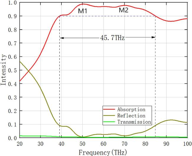
Figure 3. The absorption curve (red), reflection curve (brown) and transmission curve (green) of the absorber in the range of 20–100 THz when the Fermi level is 10 meV. |
To analyse the absorption mechanism of the absorber in depth, when the Fermi energy level is 10 meV the simulation analysis of the electromagnetic field is carried out on the two resonant peaks M1 and M2 respectively. The electric and magnetic field distributions of the absorber at the resonance frequency are calculated, and the results are shown in figures 4(a)–(d). In this figure, the electric field at point M1 is mainly concentrated at the top and bottom of the two ends of the semicircular inner-ring resonator and the bottom of the two sides of the outer-ring resonator, forming an electric dipole resonance along the Y-axis direction. The electric field at point M2 is mainly distributed near the bottom of the inner-ring resonator. It is also important to note that the magnetic dipole response of the resonator is parallel to the X-axis and perpendicular to the absorber due to the opposing magnetic fields generated on the left and right sides of the inner-ring resonator. With the superposition of two resonance modes, the electric and magnetic dipoles, the resonator achieves perfect absorption of the broad band near $50.4\,{\rm{THz}}.$ In particular, the magnetic dipole response is due to the electromagnetic coupling effect between the inner- and outer-ring structures, while the superposition of the two resonance modes, electric and magnetic dipole, is due to the structural design and material properties of the resonator. These properties enable the resonator to achieve high-efficiency absorption of electromagnetic waves with perfect absorption over a wide frequency band. Thus, in essence, the absorber actually absorbs and dissipates electromagnetic waves by confining the electric and magnetic fields within the absorber structure and utilising the phenomena of reflection, interference and coupling between the resonators.
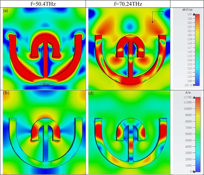
Figure 4. Distribution of electric field (a), (c) and magnetic field (b), (d) at two points M1 and M2. |
To further investigate the high absorption at the two points M1 and M2 we introduce impedance matching theory. According to impedance matching, high absorption levels can be achieved when the relative impedance Z of the wave-absorbing material is close to the impedance of free space [25]
$\begin{eqnarray}Z=\pm \sqrt{\displaystyle \frac{{\left({1+S}_{11}\right)}^{2}-{S}_{21}^{2}}{{\left(1-{S}_{11}\right)}^{2}-{S}_{21}^{2}}}.\end{eqnarray}$
Applying the parametric inversion method and equation (8 ), the relative impedance of the absorber can be calculated. Complete absorption can be achieved when the relative impedance matches that of free space. Therefore, for effective absorption, the real and imaginary parts of the relative impedance must be close to 1 and 0, respectively. The results in figure 5 show that at the peak frequency of absorption, the imaginary and real parts of the relative impedance are close to 0 and 1, respectively, which effectively explains the higher absorption at these two points. To explore the influence of tunable materials on the absorption rate, Dirac semimetallic materials and VO2 absorbers at different Fermi levels and VO2 absorbers in different states were simulated.
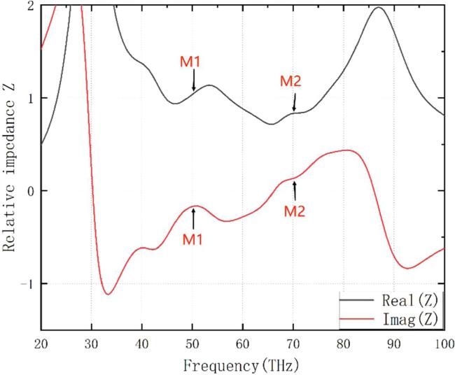
Figure 5. Relative impedance of the absorber. |
In the introduction to Dirac semimetals it was mentioned that the factors affecting the conductivity of Dirac semimetals include different Fermi levels and different temperatures; the influence of different Fermi levels on the absorption rate is mainly discussed in this work, and the influence of temperature on the conductivity of Dirac semimetals is not considered. Therefore, in this paper, a bias voltage Vg is added between the Dirac semimetal and VO2, with the Dirac semimetal as the positive electrode and the VO2 layer in the metallic state as the negative electrode [26–28], as shown in figure 6.
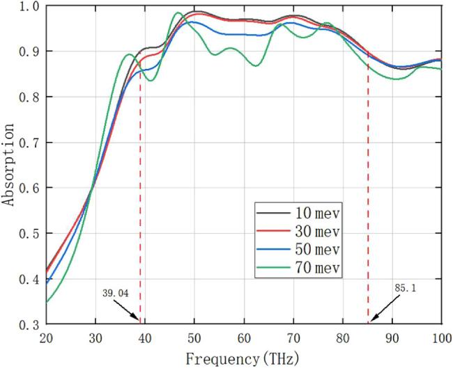
Figure 6. Effect of different Fermi energy levels on absorptivity. |
The absorbers at different Fermi levels were simulated, and the curves of the absorption rate with frequency were plotted. As can be seen from figure 6, the absorption performance of resonant waves in the 39–90 THz band decreases significantly as the Fermi level increases, which is related to the conductivity properties of the Dirac semimetal itself. As can be seen from figure 1, in the frequency range of 0–100 THz the real part of the dielectric constant of Dirac semimetallic materials decreases and the imaginary part increases with increase in frequency. The corresponding conductivity also decreases in the real part and increases in the imaginary part. It is well known that when the conductivity of a material is complex, the real part of the conductivity indicates the size of the conductivity, i.e. the strength of the conductivity of the material, while the imaginary part of the conductivity indicates the impedance of the material, i.e. the ability of the material to conduct the phase difference under the action of the electromagnetic field, and the imaginary part of the conductivity leads to a time lag of the charge inside the material and the attenuation of the electric field. The impedance of the material is larger for Dirac semimetallic materials when the frequency is higher. The Fermi level rises, the electron lifetime inside the resonator made of a Dirac semimetal decreases, the rate at which the electrons lose their energy is accelerated and the electrons in the structure are more likely to be excited, which leads to a decrease in the resonant wave performance.
VO2 materials, like photosensitive silica, are characterised by both metallic and insulating states [19, 29]: below 68 °C they are insulating and can be considered as lossless dielectrics with relative dielectric constants, while above 68 °C they are characterised as in a metallic state and their relative dielectric constant can be described according to the Drude [30] model
$\begin{eqnarray}{\sigma }_{{\mathrm{VO}}_{2}}\left(\omega \right)={\varepsilon }_{{\rm{\infty }}}-\displaystyle \frac{{\left({\omega }_{{\rm{P}}}\left({\sigma }_{{\mathrm{VO}}_{2}}\right)\right)}^{2}}{{\omega }^{2}+{\rm{i}}\gamma \omega }\,\end{eqnarray}$
where ${\varepsilon }_{\infty }=12$ is the high-frequency permittivity of VO2 and $\gamma =5.75\,\times \,{10}^{13}\,{{\rm{s}}}^{-1}$ is the damping frequency. The Dirac semimetallic plasma can be expressed as $\begin{eqnarray}{\omega }_{{\rm{p}}}^{2}\left({\sigma }_{{\mathrm{VO}}_{2}}\right)=\displaystyle \frac{{\sigma }_{{\mathrm{VO}}_{2}}}{{\sigma }_{0}}{\omega }_{{\rm{p}}}^{2}\left({\sigma }_{0}\right)\,\end{eqnarray}$
where ${\sigma }_{0}=\,3\,\times \,{10}^{5}\,{\rm{S}}\,{{\rm{m}}}^{-1}\,$ and ${\omega }_{p}\left(\omega \right)=1.4\,\times \,{10}^{14}\,\mathrm{rad}\,{{\rm{s}}}^{-1}.$ In this study, VO2 was set to be in the metallic state and the corresponding conductivity was set at 105 S m–1. To study the contribution of the VO2 layer to the absorption of the absorber, the transmittance, reflectance and absorption of the VO2 layer in the absorber were calculated. The results are shown in figures 7(a) and (b).From figure 7(a), when the VO2 layer is not set, the reflectance and transmittance of the absorber in the frequency range of 39–90 THz increase significantly. According to the formula for calculating absorption introduced above, $A\left(\omega \right)=1-R\left(\omega \right)-T\left(\omega \right),$ it can be obtained that the absorption rate of the absorber is kept below 40% when no VO2 layer is set. After setting the VO2 layer in the absorber, the reflectivity of the absorber is kept below 10% in the absorption band of 50–85.6 THz and the peak transmittance is no more than 2%, so the absorption rate can be maintained above 90% in the absorption band, as shown in figure 7(b). As can be seen in figures 7(a) and (b), the VO2 layer plays an important role in the absorption of the absorber. When a VO2 layer is provided in the structure, the reflectivity and refractive index of the absorber are greatly reduced. This is because when VO2 is in a metallic state, it is equivalent to a metallic reflective layer. When an electromagnetic wave is incident on the surface of the absorber, part of the electromagnetic wave is directly reflected to free space by the surface and the other part is dissipated through the surface into the resonant layer inside the absorber. When the electromagnetic wave through the resonance layer reaches the VO2 layer, due to the thickness of the VO2 layer being greater than a wavelength, most of the electromagnetic wave will not be able to penetrate through the VO2 layer and will be reflected back to the resonance layer to continue to dissipate; a number reflections of the electromagnetic energy inside the absorber will lead to gradual dissipation.
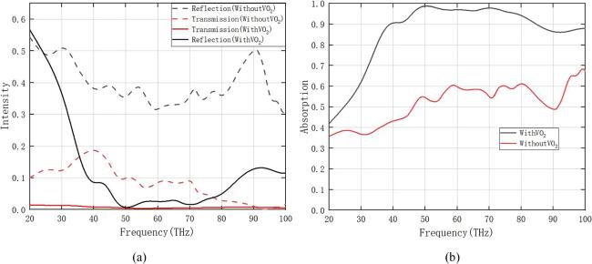
Figure 7. The effect of VO2 layer on the (a) reflectivity and refractivity and (b) the absorptivity of the structure. |
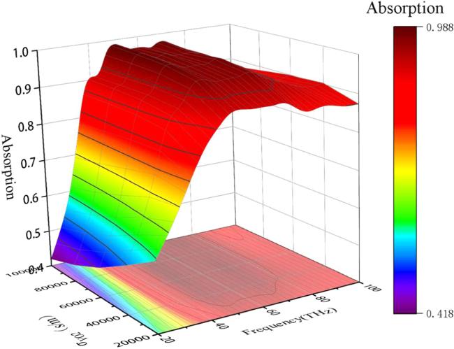
To further investigate the effect of the conductivity of VO2 on the absorption rate of the absorber, the absorption spectra of the Fermi level at $10\,{\rm{meV}}$ with different VO2 conductivities were calculated. The results are shown in figure 8. It can be seen from this figure that when the conductivity of the VO2 was increased from 0 to 10 000 S m–1 the absorption of the absorber increased rapidly with the increase in conductivity but did not show broadband absorption and the absorption remained below 80%. When the conductivity continues to increase to 80 000 S m–1 the absorption rate also increases with the increase in conductivity, but the growth rate slows down significantly, and the absorption rate remains between 80% and 90%. When the conductivity is further increased to 100 000 S m–1 the absorption rate does not change significantly with the increase of conductivity, and the absorption rate remains above 90%, showing obvious broadband absorption characteristics.
Figure 8. Absorption line spectra for different conductivities of VO2. |
5. Conclusion
In summary, this paper presents a tunable absorber based on metamaterials with high absorption frequencies in the range 35–90 THz. We have analysed the performance variation of the absorber under different conditions for optimal absorption. In addition, the effects of Dirac semimetallic materials at different Fermi energy levels and VO2 in different states on the performance of the absorber are discussed, fully demonstrating the tunable performance of the absorber. Since Dirac semimetallic and VO2 materials are used to fabricate the absorber, the absorber designed in this paper is double-tuned and more flexibly controlled than other, non-adjustable, absorbers. In addition, in the field of Dirac semimetallic absorbers, the absorber designed in this paper mainly concerns the wavelength band in the mid-infrared region, providing many areas for research into Dirac semimetallic absorbers. The development of tunable metamaterial absorbers faces higher development requirements, such as a simple structure, rich functions and accurate tuning. As metamaterials can overcome the defects of traditional materials, tunable metamaterial wave-absorbing materials can be individually designed with smaller and lighter structures, conducive to more novel electromagnetic functions and having broad application prospects in the field of wave-absorbing materials. In the future, and with continuous scientific and technological development, the related theory and manufacturing process will continue to progress and tunable metamaterial wave-absorbing materials are expected to achieve better performance and wider application.