


1. Introduction
Electromagnetically induced transparency (EIT) originally refers to the appearance of a narrow band of transmission frequencies in a medium that, in its initial state, is impermeable, due to the coherent action of a coupled beam in an atomic system [1-3]. Due to the EIT requires high-intensity laser [4], extremely low temperature [5], and demanding environment [6-8], the practical application of EIT has been somewhat limited. The plasmon-induced transparency (PIT) effect combines of EIT and surface plasmon polaritons (SPPs) [9-11]. The PIT comes from the destructive interference between the dark modes and the bright modes [12-14]. The PIT effect provides several benefits, such as the ability to function at room temperature, a sharply varying transmission spectrum, and ease of integration onto a chip. The PIT effect has become a focal point of research in many optical systems, including photonic crystal waveguide resonators [15], metal-dielectric-metal (MIM) waveguides [16], microelectromechanical systems (MEMSs) [17], subwavelength structures [18], microresonators [19], plasmonic gratings [20], three-dimensional metamolecules [21], and hybrid metal-graphene metamaterials [22]. As a result, research on the PIT effect has attracted increasing attention from researchers worldwide. For example, Wang et al proposed a triple PIT structure based on two big bright modes for sensing [23]. Yahiaoui et al presented a broadband EIT based on a subwavelength structure with broken symmetry [24]. The structure can trigger the quintuple PIT effect. The structure has a high group index. Meng et al designed a composite structure of horizontal and vertical graphene strips [25]. The structure can induce a triple PIT effect through the coupling of three bright modes and one dark mode.
Metamaterials are artificially engineered on-demand materials that do not occur naturally and are designed to have specific properties. They are usually composed of periodically arranged subwavelength structures, which can manipulate electromagnetic waves in unique ways. Metamaterials manipulate electromagnetic waves for extraordinary applications such as the creation of Quasi-Bound States [26-28], and various sensors [29,30]. Therefore, metamaterials have garnered significant attention from researchers in fields such as physics, materials science, optics, and chemistry [31]. The discovery of graphene has led to a surge in research on two-dimensional (2D) layered materials and mixed-dimensional heterostructure. Different from graphene material, when transition metal binary compounds (e.g., ${{\rm{MoS}}}_{2}$, ${{\rm{MoSe}}}_{2}$, ${{\rm{WS}}}_{2}$, and ${{\rm{WSe}}}_{2}$) are transformed from macrostructures to 2D monolayer structures, they become direct bandgap semiconductors. The monolayer ${{\rm{MoS}}}_{2}$, which has a direct bandgap of about 1.8 eV particularly [32], emits light intensely and aids the excitation of electrons. So, it has been regarded as the preferred atomically thin material for photodetection [33], photocatalysis [34,35], as well as photovoltaic devices [36]. However, despite the great potential of ${{\rm{MoS}}}_{2}$ in photonics and optoelectronic applications, the light-matter interaction is significantly hindered due to its intrinsic atomic thickness, leading to extremely low light emission and absorption [37]. There is limited systematic research on the PIT effect of ${{\rm{MoS}}}_{2}$. Nevertheless, the PIT effect is also important for applications in high-sensitivity sensors and slow-light sensors.
In this paper, the PIT effect is realized based on a composite ${{\rm{MoS}}}_{2}$ structure. The designed unit cell consists of a monolayer ${{\rm{MoS}}}_{2}$ made up of cross-shaped and square-shaped structures. The PIT effect results from the near-field coupling between two bright modes. We further discussed the resonance mechanism of the destructive interference in ‘bright-bright' modes concerning the electric field distributions. With Finite-Difference Time-Domain (FDTD) simulations, the relationship between the coupling distance and angle between the cross-shaped and square structures was investigated, along with the effects of carrier concentration in ${{\rm{MoS}}}_{2}$. A Lorentzian mode theory model is used to fit the coupling between different modes, and the fitting effect is excellent. When the proposed structure is used as a refractive index sensor, the sensitivity and FOM are $0.98\,{\rm{THz}}\,{{\rm{RIU}}}^{-1}$ and $1.10\,{{\rm{RIU}}}^{-1}$, respectively. Finally, the sensor exhibits a good slow light property, and its group delay is about $0.52\,{\rm{ps}}$. Therefore, we believe that this design has broad application prospects in fields such as optical sensors, slow light devices, and flexible THz functional devices.
2. Design and simulation
To investigate the transmission performance of the bright-bright mode PIT (BB-PIT) based on the ${{\rm{MoS}}}_{2}$ metamaterial, a periodic structure is proposed. figure 1(a) shows a three-dimensional (3D) array schematic diagram of the proposed sensor. The plane waves are incident from the top and the electric vector is pointed to the y direction. The periodic dimensions of each direction are set as the same size: $Px=Py=P=60\,{\rm{\mu }}{\rm{m}}$. It is also clear to observe that the device consists of a square cross structure and a dielectric layer. In many optoelectronic device designs, TOPAS polymer was selected due to its low loss in THz frequency band, in this paper, the constant refractive index (RI) of TOPAS is 1.53 [38] and its thickness is $h=30\,{\rm{\mu }}{\rm{m}}$. To better describe the geometrical parameters, the vertical view is shown in figure 1(b). The length of the cross shape is ${l}_{1}=32\,{\rm{\mu }}{\rm{m}}$, the width of the cross shape is ${w}_{1}=3\,{\rm{\mu }}{\rm{m}}$, the length of the square resonator is ${l}_{2}=40\,{\rm{\mu }}{\rm{m}}$ and the width of the square resonator is ${w}_{2}=3\,{\rm{\mu }}{\rm{m}}$. The air gap between the ring and the cross resonators is about $1\,{\rm{\mu }}{\rm{m}}$, such a small air gap will result in strong near-field coupling strength. In the THz frequency domains studied in this paper, the intraband transition in monolayer ${{\rm{MoS}}}_{2}$ plays a major role, the surface conductivity can be calculated by the Drude model [39,40],
$\begin{eqnarray}\sigma \left(\omega \right)={\rm{i}}\displaystyle \frac{n{{\rm{e}}}^{2}}{{m}^{* }\left(\omega +{\rm{i}}{\rm{\Gamma }}\right)},\end{eqnarray}$
where ω is the angular frequency of the incident wave, ${\rm{\Gamma }}$ is the damping constant which is inverse to the intrinsic relaxation time, the intrinsic relaxation time is set $\tau =0.17\,{\rm{ps}}$ in this model [40]. For n-type doped ${{\rm{MoS}}}_{2}$ material, the effective electron mass is about ${m}^{* }=0.53{m}_{e}$, n and e are the carrier concentration and electron mass. One major advantage of ${{\rm{MoS}}}_{2}$ based optoelectronic devices is that their conductivity can be adjusted through bias voltage [41].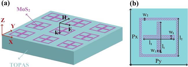
Figure 1. (a) A 3*3 periodic array of the structure in 3D view; (b) top view of the periodic unit cell. The geometric parameters are as follows: ${l}_{1}=32\,{\rm{\mu }}{\rm{m}}$, ${w}_{1}=3\,{\rm{\mu }}{\rm{m}}$, ${l}_{2}=40\,{\rm{\mu }}{\rm{m}}$, ${w}_{2}=3\,{\rm{\mu }}{\rm{m}}$, $h=30\,{\rm{\mu }}{\rm{m}}$, $P=60\,{\rm{\mu }}{\rm{m}}$. |
In this study, the transmission characteristics and field distributions were calculated using MATLAB, Origin, and FDTD solution. During the simulation, the positive incident light in the polarization mode of transverse magnetic (TM) (electric field E parallel to the x direction) is selected and projected vertically onto the structure. Periodic boundary conditions (PBCs) are used in x and y directions, and the perfect matching layers (PMLs) are adopted in the z-direction, the number of PMLs in the proposed study is set to be 8, where the reflection coefficient is smaller than 10-6, the spatial mesh sizes are set to ${\rm{\Delta }}x={\rm{\Delta }}y=0.5\,{\rm{\mu }}{\rm{m}}$, ${\rm{\Delta }}z=0.3\,{\rm{\mu }}{\rm{m}}$. It is noteworthy that the incident light source was positioned in the air, characterized by an ambient refractive index of $n=1$. Two monitors (record transmission and reflection coefficients) are placed at a distance of $40\,{\rm{\mu }}{\rm{m}}$ from the surface of the device, and the incident light source is placed above the substrate at a distance of $5\,{\rm{\mu }}{\rm{m}}$. To avoid calculation errors, the total simulation time is $100000\,{\rm{fs}}$. The equivalent permittivity of monolayer ${{\rm{MoS}}}_{2}$ ${\varepsilon }_{m}$ was calculated by the conductivity as [42].1 ) and (2 ), the conductivity and permittivity of monolayer ${{\rm{MoS}}}_{2}$ can be obtained, as shown in figure 2, the real and imaginary parts of ${\varepsilon }_{m}$ under different carrier concentrations are calculated. We can notice the permittivity of monolayer ${{\rm{MoS}}}_{2}$ increases with the carrier concentration. Similar to graphene material, the n-doped ${{\rm{MoS}}}_{2}$ material behaves similar to metallic materials [43]. Therefore, similar to graphene, the ${{\rm{MoS}}}_{2}$-strong SPP mode can also be tune by the carrier concentration, then transmission and absorption performance of the device can be controlled.
$\begin{eqnarray}{\varepsilon }_{m}=1+\displaystyle \frac{{\rm{i}}\sigma }{\omega {\varepsilon }_{0}{t}_{m}},\end{eqnarray}$
where ${\varepsilon }_{0}$ is the permittivity of the vacuum. According to formula (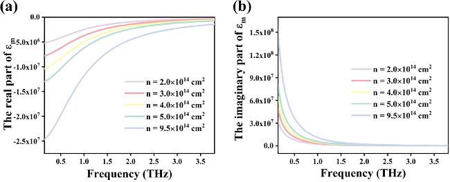
Figure 2. (a) The real part of the permittivity of the monolayer ${{\rm{MoS}}}_{2}$ with varying carrier concentrations; (b) the imaginary part of the permittivity of monolayer ${{\rm{MoS}}}_{2}$ with varying carrier concentrations. |
3. Result and discussion
The red curve in figure 3(a) shows the calculated transmission spectrum under the TM-polarization. We can notice two transmission dips at corresponding resonance frequencies of 1.65 THz (marked by Dip1) and 3.16 THz (marked by Dip2) and one transmission peak at the corresponding resonance frequency of 2.42 THz (Peak). In the following, a Lorentzian mode theory model is used to fit the coupling effect between the two different modes [44,45].
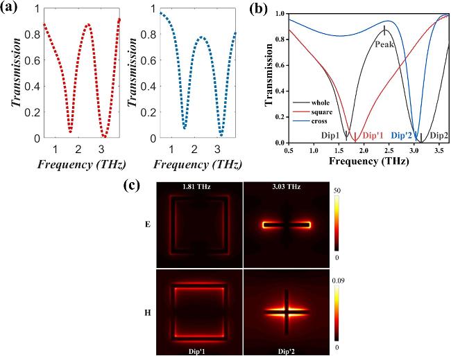
Figure 3. (a) The transmission spectra of the FDTD simulation (red solid line) and theory spectrum (blue solid line); (b) the transmission spectra with three different structures; (c) the electric field distributions corresponding to different structures. |
Here, the incident electric field is $E={E}_{0}{{\rm{e}}}^{j\omega t}$. Then, the model can be described by the following two equations3 ) and (4 ), combined with (5 ) and (6 ), The effective electric susceptibility of the modes can be derived as7 ) and (8 ), the transmission spectrum of the ${{\rm{MoS}}}_{2}$-based THz metasurface can be derived. The simulation results and theoretical fittings are presented in figure 3(a). It can be observed that the theoretical results are in good agreement with the simulation outcomes.
$\begin{eqnarray}{\ddot{x}}_{1}(t)+{\gamma }_{a}{\dot{x}}_{1}(t)+{\omega }_{1}^{2}{x}_{1}(t)+{\kappa }^{2}{x}_{2}(t)={q}_{1}{E}_{0},\end{eqnarray}$
$\begin{eqnarray}{\ddot{x}}_{2}(t)+{\gamma }_{b}{\dot{x}}_{2}(t)+{\omega }_{2}^{2}{x}_{2}(t)+{\kappa }^{2}{x}_{2}(t)={q}_{2}{E}_{0},\end{eqnarray}$
where, $({x}_{1},{x}_{2})$, $({\omega }_{1},{\omega }_{2})$, and $({q}_{1},{q}_{2})$ are the displacements, resonant frequencies, and coupling strength coefficients with THz waves, respectively. $({\gamma }_{a},{\gamma }_{b})$ are the loss terms associated with the metasurface structures which are closely to ${\gamma }_{1}$ and ${\gamma }_{2}$ for each individual metasurface structure. In addition, and ${\gamma }_{b}=({\gamma }_{2}-{\gamma }_{1})/2$. To better align with our model, phase information $\phi $ has been incorporated [46]. The $\kappa $ represents the coupling strength with loss, and the energy loss during the transfer from one cross shape to the square frame. $\kappa $ can be calculated using the following formula $\begin{eqnarray}\kappa =g-{\rm{i}}\sqrt{{\gamma }_{a}{\gamma }_{b}}{{\rm{e}}}^{{\rm{i}}\phi },\end{eqnarray}$
where, g represents the coupling strength between two bright modes, and Φ can be written as $\begin{eqnarray}\phi =\left({\phi }_{1}-{\phi }_{2}\right)\left({\omega }_{1}+{\omega }_{2}\right)/2.\end{eqnarray}$
By solving equations ( $\begin{eqnarray}\begin{array}{lll}{\chi }_{\mathrm{eff}} & =& \displaystyle \frac{K}{{{P}_{1}}^{2}{P}_{2}}\left(\displaystyle \frac{{P}_{1}\left({P}_{2}+1\right){\kappa }^{2}+{{P}_{1}}^{2}\left({\omega }^{2}-{{\omega }_{2}}^{2}\right)+{P}_{2}\left({\omega }^{2}-{{\omega }_{1}}^{2}\right)}{{\kappa }^{4}-\left({\omega }^{2}-{{\omega }_{1}}^{2}+{\rm{i}}\omega {\gamma }_{a}\right)\left({\omega }^{2}-{{\omega }_{2}}^{2}+{\rm{i}}\omega {\gamma }_{b}\right)}\right.\\ & & \left.+{\rm{i}}\omega \displaystyle \frac{{{P}_{1}}^{2}{\gamma }_{b}+{P}_{2}{\gamma }_{a}}{{\kappa }^{4}-\left({\omega }^{2}-{{\omega }_{1}}^{2}+{\rm{i}}\omega {\gamma }_{a}\right)\left({\omega }^{2}-{{\omega }_{2}}^{2}+{\rm{i}}\omega {\gamma }_{b}\right)}\right),\end{array}\end{eqnarray}$
where, the $K$ is the proportionality factor of the ${{\rm{MoS}}}_{2}$-based THz metasurface, ${P}_{1}$ is the ratio of coupling strength coefficients with incident waves in single structure, and ${P}_{2}$ is the ratio of effective mass between the two structures. Moreover, the transmission T is $\begin{eqnarray}T=1-\rm{Im}\left({\chi }_{\mathrm{eff}}\right).\end{eqnarray}$
By combining with (To explain the contribution of each component, the transmission spectra of the individual components and the hybrid components are shown in figure 3(b). We can find that, both the cross-shaped and square structures of the metasurface can exhibit a bright mode under the excitation of an electromagnetic wave in TM-polarization. Two resonant frequencies are different because the physical dimensions of the two MoS2 structures are different. For a single square structure, as shown in figure 3(b), we can notice a transmission valley located at 1.81 THz (marked by mode B), the square structure resonator can be directly excited by the input electromagnetic wave, which can be seen as a bright mode. The field pattern of 1.81 THz is depicted in figure 3(c), and we can observe that a strongly localized surface plasmon resonance (LSPR) is excited, and a dipole resonance mode is excited along the x direction. For a single cross-shaped structure, as shown in figure 3(b), we can notice a transmission valley located at 3.03 THz (marked by mode C). The electric and magnetic field distribution of 3.03 THz is shown in figure 3(c), and we can observe a strong dipole plasmon resonance excited at the two ends of the horizontal arm. Thus, the cross-shaped structure can be seen as another bright mode. It is evident that both sub-resonators exhibit transmission characteristics of a single dip. So we can know that, a metasurface can generate BB-PIT under the excitation of electromagnetic waves when the two structures are combined. The PIT transmission peak at a frequency of 2.42 THz is located between transmission Dip1 (1.65 THz) and Dip2 (3.16 THz). These two dips approaching consensus to the frequencies of modes B and C. Due to the presence of weak coupling, the resonance frequencies of the coupled structure do not precisely match the results obtained when each sub-resonator is simulated individually.
To reveal the physical mechanism of the PIT spectrum, the electric field distribution and magnetic field distribution of the corresponding two dips and peak are depicted. As shown in figures 4(a) and (d), we can observe that the electric field is distributed at the two ends of the cross resonator, a part of energy is confined at the left and right sides of the square resonator. The amplitude of a magnetic field is two orders of magnitude smaller than that of an electric field, so we mainly analyze the electric field. For the transmission peak, as exhibited in figures 4(b) and (e), the electric field is more localized in the air gap between the cross and square resonators. figures 3(c) and (f) exhibit the field distribution of Dip2, we can notice the electric field is totally concentrated at the two ends of the cross resonator. Therefore, we can conclude that the destructive effect between the bright modes supported by the two substructures leads to the appearance of the PIT spectral line.
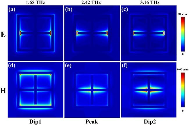
Figure 4. Electric field distributions and magnetic field distributions in the x-y plane at different frequencies (a), (d) 1.65 THz; (b), (e) 2.42 THz; (c), (f) 3.16 THz. |
In order to study the effect of structural parameters on the PIT of the ${{\rm{MoS}}}_{2}$-based THz metasurface. The parameters of the cross-shaped and square structures were changed respectively, and the results are shown in figure 5. As shown in figure 5(a), the effect of the length of the cross ${l}_{1}$ on the PIT spectrum is studied by the controlling variable method. We can observe that the PIT window gradually decreases when increasing the size of ${l}_{1}$. The resonant frequencies of Dip2 and Peak exhibited a red shift with different degrees, the change of Dip1 is relatively weak, it is not difficult to see from the previous field diagram that ${l}_{1}$ has a greater impact on Dip2. The impact of the cross width ${w}_{1}$ on the PIT spectrum is analyzed, as illustrated in figure 5(b). We can see that the PIT window gradually increases with increasing size of ${w}_{1}$. The resonant frequencies of Dip1 and Peak exhibited a slightly red shift with different degrees, and the change of Dip2 is weak, causing an increase in the width of the PIT spectrum. As shown in figure 5(c), the effect of the width of the square ${l}_{2}$ on the PIT spectrum is analyzed. We can observe that the PIT window gradually increases with the increasing size of ${l}_{2}$. The resonant frequencies of Dip1 exhibited a red shift while the changes of Peak and Dip2 can be ignored, this pattern of change is consistent with the field diagram, since the size of the square resonator is related to the first transmission dip. The impact of the square width ${w}_{2}$ on the PIT spectrum is analyzed, as illustrated in figure 5(d). We can observe that the PIT window gradually decreases with increasing the size of ${l}_{2}$. The resonant frequencies of Dip1 exhibited a blue shift while the changes of Peak and Dip2 can be ignored. Moreover, we also investigated the effect of variations in the height of the TOPAS dielectric $h$ and structural period $P$ on the transmission spectrum, as depicted in figures 5(e) and (f). The variations in both factors have a minimal impact on the transmission spectrum. In the end, we determine that the optimal parameter of $h$ is $h=30\,{\rm{\mu }}{\rm{m}}$ and $P$ is $P=60\,{\rm{\mu }}{\rm{m}}$. Therefore, we can tune the width of the PIT window by changing the parameter sizes of cross and square structures.
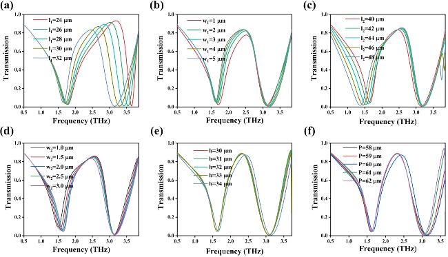
Figure 5. The transmission spectra with different structural parameters: (a) ${l}_{1}$ is allowed to change; (b) ${w}_{1}$ is allowed to change; (c) ${l}_{2}$ is allowed to change; (d) ${w}_{2}$ is allowed to change; (e) h is allowed to change; (f) $Px=Py=P$ is allowed to change. |
In addition, the effect of the cross-angle was also investigated. The cross-angle is the angle between the arm of the cross resonator and the horizontal direction. As shown in figures 6(a)-(c), the schematic diagrams and simulation spectra of several cross angles are depicted. The first image in figure 6(a) illustrates the structure we proposed, corresponding to the case when the angle $\alpha =0^\circ $. As shown in figure 6(b), when $\alpha =30^\circ $, $\alpha =45^\circ $ or $\alpha =60^\circ $, we can observe when $\alpha =0^\circ $, the peak of PIT is the highest because in this case, the minimum coupling distance between the two substructures results in the maximum coupling strength. From figure 9(c), we can see that at the angle $\alpha =0^\circ $, the electric field energy is more concentrated and focused at the air gap between the two substructures. When $\alpha =30^\circ $, $\alpha =45^\circ $ or $\alpha =60^\circ $, the electric dipole resonance mode is still excited by the two arms of the cross structure, the PIT spectral lines can still be maintained well. When $\alpha =60^\circ $, as the two arms of the cross resonator move closer to the upper and lower sides of the square resonator, the four inner edges of the square structure can be weakly excited, compared with the local fields on the left and right sides, the electric fields on the upper and lower inner sides of the square structure are relatively stronger. This asymmetric coupling causes the PIT peak shift towards higher frequency, the PIT spectral lines become asymmetric, similar to the Fano resonance spectral lines. Therefore, the above result demonstrates that the proposed structure possesses significant production errors to ensure the stability of the PIT spectrum.
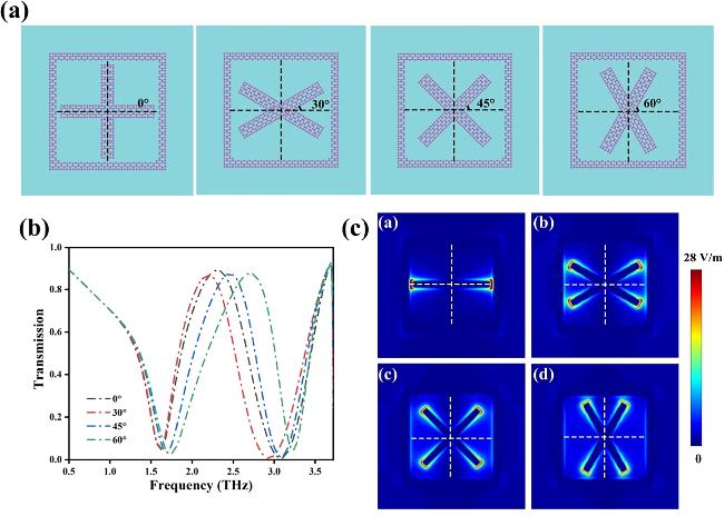
Figure 6. (a)-(c) The schematic diagrams under the conditions of different angles of intersection; (d) absorption spectra of the absorber under the conditions of different angles of intersection; (e)-(g) the distributions of electric fields |E| in the y-z planes through the center of the cross under the conditions of different angles of intersection. |
From the above discussion, we understand that the transmission response can be tuned by controlling the carrier concentration of ${{\rm{MoS}}}_{2}$. We compared the transmission spectra with different carrier concentrations and the condition of an uncoated monolayer ${{\rm{MoS}}}_{2}$, as shown in figure 7. Obviously, in the absence of monolayer ${{\rm{MoS}}}_{2}$, the absorptivity is about 0. The black curve (without ${{\rm{MoS}}}_{2}$) represents that the incident THz wave can easily be transmitted. As the carrier concentration increases, the PIT window expands, and the transmission spectrum exhibits a blue shift. Hence, it further illustrates that the PIT width and resonance frequency can be adjusted by controlling the carrier concentration. figure 8 shows the FDTD simulated spectra and theoretical fitted spectra with different carrier concentrations. We can observe the simulation results are generally consistent with the theoretical calculations.
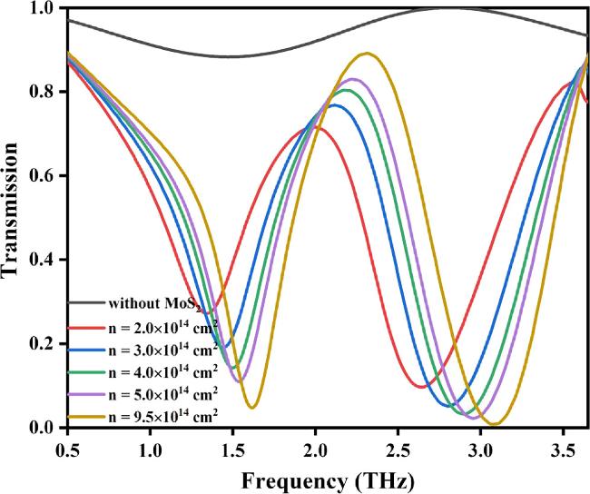
Figure 7. Absorption spectra of the absorber under the conditions of uncoated monolayer ${{\rm{MoS}}}_{2}$ and different carrier concentrations from $n=1.0\times {10}^{14}\,{{\rm{cm}}}^{-2}$ to $n=9.5\times {10}^{14}\,{{\rm{cm}}}^{-2}$. |
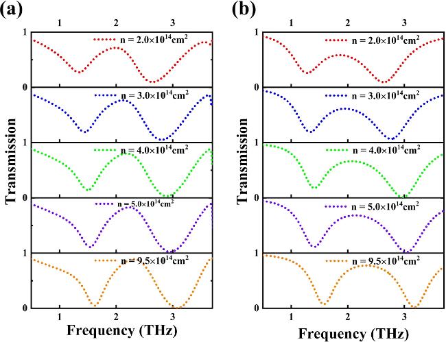
Figure 8. The FDTD simulated and theory fitted spectra with different carrier concentrations. |
Additionally, the proposed structure has significant research value in the sensing direction, and the analysis of its sensing principles is as follows: with the incident THz wave, the surface plasmon polariton (SPP) resonance is generated at the interface of the monolayer ${{\rm{MoS}}}_{2}$ and TOPAS. To further investigate the RI sensitivity of the proposed structure, the transmission performances of analytes with refractive indices ranging from 1 to 1.4 are depicted. The frequency shifts with different refractive indices are shown in figure 9(a). With the increasing refractive index, the frequency of peak is shifted from 2.42 THz to 2.03 THz. The correlation coefficients of dips and peaks are ${{R}_{1}}^{2}=0.9963$, ${{R}_{2}}^{2}=0.9957$ and ${{R}_{3}}^{2}=0.9977$, respectively. This indicates that the shifts of dips and peaks can be approximated as a linear shift. The good linear relationship between the resonance frequency and the refractive index indicates that the proposed ${{\rm{MoS}}}_{2}$-based metamaterial can be used for sensing applications. The sensitivity S stands for the frequency shift caused by the change in the refractive index per unit, which can be calculated by [47]
$\begin{eqnarray}S=\displaystyle \frac{{\rm{\Delta }}\lambda }{{\rm{\Delta }}n}.\end{eqnarray}$
The S values of the Dip1, Peak, and Dip2 are $0.48\,{\rm{THz}}\,{{\rm{RIU}}}^{-1}$, $0.98\,{\rm{THz}}\,{{\rm{RIU}}}^{-1}$, and $0.78\,{\rm{THz}}\,{{\rm{RIU}}}^{-1}$, respectively. The S of the peak is the biggest, this is because for the PIT peak, the surface of ${{\rm{MoS}}}_{2}$ has a stronger electric field density, which is more sensitive to the changes of the analyte. The sensor performance is also evaluated using the figure of merit (FOM), which can be defined as [48] $\begin{eqnarray}{\rm{F}}{\rm{O}}{\rm{M}}=\displaystyle \frac{S}{{\rm{F}}{\rm{W}}{\rm{H}}{\rm{M}}}.\end{eqnarray}$
figure 9(b) shows the FOM values of Dip1, Peak, and Dip2 are $0.54\,{{\rm{RIU}}}^{-1}$, $1.10\,{{\rm{RIU}}}^{-1}$ and $0.88\,{{\rm{RIU}}}^{-1}$, respectively. As a reference, we compare the sensing performance with other studies in table 1. We can observe that the proposed sensor possesses a wider working band and a relatively better of S. The quality factor Q can be calculated by FWHM and the resonance wavelength. $\begin{eqnarray}Q=\displaystyle \frac{f}{{\rm{F}}{\rm{W}}{\rm{H}}{\rm{M}}}.\end{eqnarray}$
Table 1. Performance comparisons of the proposed PIT metamaterial structure with other similar structures. |
| References | Materials | Working band | Window properties | Sensitivity-max | FOM-max | Group delay-max |
|---|---|---|---|---|---|---|
| [51] | ${\rm{CNTs}},{\rm{Si}}$ | 0.6-2.5 THz | Single | 0.74 THz RIU-1 | 0.54 ps | |
| [52] | ${\rm{CNTs}},{\rm{polymide}}$ | 0.6-1.2 THz | Single | 0.32 THz RIU-1 | 2.12 ps | |
| [53] | ${\rm{Graphene}},{{\rm{SiO}}}_{2},{\rm{Si}}$ | 0.3-1.8 THz | Single | 0.34 THz RIU-1 | 3.60 ps | |
| [54] | ${\rm{Graphene}},{\rm{dielectric}}$ | 30-75 THz | Single | 0.36 ps | ||
| [55] | ${\rm{Graphene}},{{\rm{SiO}}}_{2}$ | 1-7 THz | Single | 1.34 THz RIU-1 | ||
| [56] | ${\rm{CNTs}},{\rm{Si}},{\rm{sapphire}}$ | 0.6-2.5 THz | Double | 1.12 THz RIU-1 | 5.77 RIU-1 | 1.71 ps |
| [57] | ${\rm{Graphene}},{\rm{Gold}}{,{\rm{SiO}}}_{2}$ | 0.3-1.3 THz | Single | 0.19 THz RIU-1 | 2.94 ps | |
| [58] | ${\rm{Gold}},{\rm{Substrate}}$ | 0.4-1.2 THz | Double | 0.14 THz RIU-1 | ||
| Our work | ${{\rm{MoS}}}_{2},{\rm{TOPAS}}$ | 0.5-3.7 THz | Single | 0.98 THz RIU-1 | 1.10 RIU-1 | 0.52 ps |
Figure 9(b) also shows the relationship between Q and the refractive index. We can notice the maximum Q-factor is 2.72. The results illustrate that the sensor exhibits a good sensing performance during the detection process in the terahertz region.
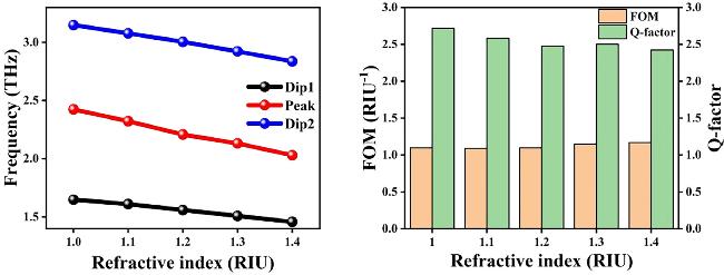
Figure 9. (a) The relationship between the resonant frequency and the refractive index. (b) the relationship between environment refractive index, FOM, and quality factor (Q-factor). |
Finally, it is well known that a key characteristic of PIT response is the strong phase dispersion within the transparent window region, which leads to a reduction in the group velocity [49]. After obtaining the phase shift $\varphi $ of the transmission spectrum, the group delay (${\tau }_{g}$) can be calculated using the following equation
$\begin{eqnarray}{\tau }_{g}=-{\rm{d}}\varphi /{\rm{d}}\omega ,\end{eqnarray}$
where $\omega $ indicates the resonant frequency. The curves of $\varphi $ and ${\tau }_{g}$ are presented in figure 10. It can be observed that the phase mutation occurs and the phase dispersion occurs at the position of the transparent window, which results in a significantly enhanced group delay. At the frequency of transparent Dip1, the group delay can reach $0.52\,{\rm{ps}}$. The delay bandwidth product (DBP) is defined as the product of maximum group delay and the spectrum bandwidth ($\mathrm{DBP}={t}_{g}\times \mathrm{FWHM}$). DBP is a figure of merit to determine the efficiency of the devices for telecommunication channels, where the maximum DBP implies that the device is more efficient to store and transmit the information through the signal channel. The calculated DBP for the proposed structure is about 0.76. In contrast other paper [50], that experimentally obtains delay bandwidth product (DBP) for selectively reconfigurable coupled-mode resonators THz MEMS metamaterial is only 0.32. It means our structure is more efficient to store and transmit the information through the signal channel. The proposed ${{\rm{MoS}}}_{2}$-based metamaterial can be obtained by chemical vapor deposition (CVD) methods [59]. First, the TOPAS substrate can be deposited by physical vapor deposition. Then, the ${{\rm{MoS}}}_{2}$ layer grown by chemical vapor deposition is transferred onto the TOPAS substrate, and then patterned into square cross arrays using electron-beam lithography followed by oxygen plasma etching [54,60]. According to the paper [41,61], the structure designed in this article is feasible.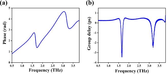
Figure 10. (a) Phase difference of the PIT spectrum; (b) group delay of the PIT spectrum. |
4. Conclusion
In this paper, we propose a PIT structure based on the ${{\rm{MoS}}}_{2}$ metamaterial. By analyzing each component and the electric field distributions, we found that the PIT effect is originated from the bright-bright mode coupling. The theoretical analysis using the Lorentzian model effectively verified the FDTD simulation results. We investigate the relationship between the coupling distance and angle between the cross-shaped and square structures, along with the effects of carrier concentration in ${{\rm{MoS}}}_{2}$. The effect of background refractive index on the PIT spectrum is analyzed in detail. Besides, the PIT curve can be applied in sensing and slow light. The maximum sensitivities and time delay of the proposed structure are $1.10\,{{\rm{RIU}}}^{-1}$, and $0.52\,{\rm{ps}}$, respectively. For telecommunication channels, the excellent value of DBP is about 0.76. In a word, this paper provides insights for future research on the PIT effect in TMDCs.
Declaration of interest statement
We declare that we have no financial or personal relationships with other people or organizations that can inappropriately influence our work, there is no professional or other personal interest of any nature or kind in any product, service and/or company that could be construed as influencing the position presented in, or the review of, the manuscript entitled, “Plasmon-induced transparency based on a molybdenum disulfide film terahertz metasurface for sensing applications”.
Funding
This work is supported by the National Natural Science Foundation of China (Grant Nos. 12075036, 12375008). Hubei Provincial Natural Science Foundation Innovation Group Project (Grant No. 2023AFA025). The Open Foundation Project of Hubei Key Laboratory of Optical Information and Pattern Recognition, Wuhan Institute of Technology.
Data availability statement
The data that supports the findings of this study is available upon reasonable request from the authors.
Authorship contribution statement
YW: Investigation, conceptualization, methodology, software, formal analysis, writing—original draft, writing—review & editing. FC: Investigation, methodology, software, formal analysis, writing—original draft, writing—review & editing, funding acquisition. WY: Supervision, formal analysis, writing—review & editing. ZY: Supervision.