


1. Introduction
Metamaterials, as an artificial synthetic material, exhibit outstanding physical properties that are completely different from natural materials [1,2]. They can show extraordinary physical properties such as negative dielectric constant [3], the electromagnetic induced transparency [4] and the electromagnetic radar stealth [5]. The microstructure of metamaterials can control the scattering of incident light in a specific way and produce a strong coupling effect with electromagnetic waves at resonant frequencies [6,7] to enhance the performance of terahertz absorbers. The use of metamaterial absorbers (MMA) in terahertz devices has broad prospects, leading to strong interest among researchers from various fields in metamaterial absorbers. In 2008, Landy et al [8] first introduced the concept of metamaterial absorbers, and since that time, the field has undergone rapid development, with applications covering multiple aspects such as sensor technology, imaging technology, and stealth technology [9-12]. The traditional MMA structure usually consists of metal-medium-metal structure, but this design has certain defects, once it is made, its operating frequency band is difficult to adjust, which greatly limits its application range and causes inconvenience to practical use [13]. Therefore, designing an absorber that has a wide absorption bandwidth characteristic and is dynamically adjustable is crucial, and graphene can solve this problem.
Graphene, a unique emerging material based on carbon, showcases a two-dimensional honeycomb structure consisting of a single layer formed by sp2 hybridized carbon atoms. It is known to be the thinnest material while possessing excellent electrical and thermal conductivity, as well as the highest optical transmittance. Its unique structure enables it to perform well in various fields such as optics and electronics [14-17]. The dielectric properties of graphene are affected by the Fermi energy, which can be regulated through chemical doping or bias voltage, thus, tunable graphene-based absorption devices can adjust the absorption band [18]. The research on graphene based terahertz metamaterial absorbers has aroused the interest of many scholars. Huang et al have developed a new type of wideband adjustable terahertz metamaterial absorber, which has achieved the adjustment of the absorption peak of MMA from 0.85 to 1.01 THz, and from 2.84 THz to 3.37 THz [19]. He et al designed a graphene-SiO2-silicon dielectric-metal ground plane structure, in which the resonance amplitude can reach 60%, and the frequency modulation depth is more than 30% [20]. Vasic and Gajic jointly found that graphene has the ability to regulate the absorption spectrum of metamaterial absorbers, achieving precise control of its absorption characteristics [21]. In addition, there is a lot of work that has confirmed the function of graphene metamaterials in the absorption spectrum tuning [22-25]. Therefore, graphene has a bright development prospect in the design field of tunable broadband artificial electromagnetic material absorbers.
This article describes a tunable broadband polarization insensitive absorber based on graphene. The metamaterial absorption unit design adopts a sandwich structure, consisting of a gold bottom layer, a silicon dioxide middle layer with a dielectric property of 1.56, and a single-layer graphene top layer. In the frequency range of 2.78 to 7.14 THz, its absorption efficiency is over 90%, exhibiting an absorption bandwidth of 4.36 THz and an average absorption efficiency of 96.1%, of which, the absorption rate exceeds 99% at 4.1-4.54 (0.44) THz, and it is noteworthy that the perfect absorption is achieved at 4.32 THz. The absorption properties of graphene materials can be improved by optimizing various geometric parameters. The absorption rate and absorption frequency band can be adjusted by adjusting the thickness of the intermediate dielectric layer. By calculating the relative impedance through parameter inversion, it is obvious that the absorber follows the principle of impedance matching. By examining the distribution of the electric field, the absorption mechanism is elucidated. By studying different polarization modes and incidence angles, it is revealed that it is insensitive to polarization due to structural symmetry, and it is found that it has low sensitivity at incidence angles. The absorption performance of the absorber at different relaxation times is compared and explained by the carrier absorbed by the plasma oscillation. The absorber possesses several advantages, including: bandwidth, high absorption rate, polarization insensitivity, simple structure, etc. These characteristics make it have a strong application prospect in many fields.
2. Structure design and simulation
The cyclic structure of the graphene absorber shown in figure 1(a) presents a sandwich design. The metal layer can enhance the local electromagnetic field through the surface plasmon resonance phenomenon, and also enhance the reflection. The refractive index of the dielectric layer can affect the resonance frequency, optimize the light absorption, and it also helps to increase the bandwidth of the absorber. Graphene can work synergistically with metal layers to participate in the surface plasmon resonance phenomenon, further enhancing absorption. The bottom layer is a base layer made of gold, with a thickness of 0.5 μm, which effectively preventing the propagation of terahertz waves below the absorption layer. The intermediate layer is a silicon dioxide (SiO2) dielectric layer, with a permittivity of 1.56 [26]. The top layer of the absorption unit structure consists of a single graphene layer, and its geometric parameters are shown in figure 1(b), period p=27 μm, dielectric layer thickness H2=13 μm. We divide the structure of graphene layer into three different parts, named region 1, region 2, and region 3. As shown in figure 4(a), region 1, a circle, radius W3=4.8 μm. In region 2, a rectangle slices off a circle from the center, and a rectangle slices off horizontally and vertically with dimensions L1=20 μm, W2=7 μm, W1=1 μm. In region 3, a large rectangle is sliced off a small rectangle with dimensions P=27 μm and L1=20 μm. The model we propose is easy to make using current technology. We first deposited a gold film on the silicon wafer, and then we deposited a layer of silica on the gold film using plasma enhanced chemical vapor deposition technology. Finally, we place the graphene sheet on top of the dielectric layer and use the electron beam lithography system to generate the pattern. In this article, the absorption membrane described was simulated using CST Microwave Studio software [27-29]. When simulating CST calculation, we choose adaptive mesh to maximize the accuracy of calculation. The absorption membrane unit exhibits consistent periodic characteristics in both the x and y directions.
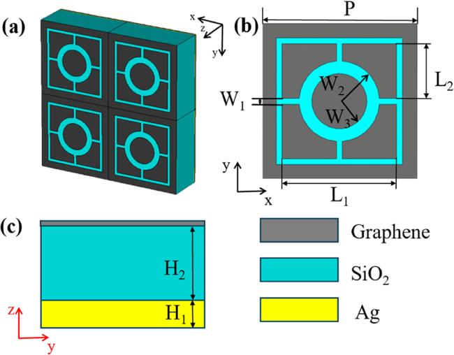
Figure 1. Periodic structure of graphene absorber (a). Top view of the absorber unit structure (b). Side view of the absorber unit structure (c). |
The surface electrical conductivity of graphene, denoted as σg, can be calculated using the Kubo formula [30], the conductivity [31] is described by the inter-band and in-band contributions, expressed as equation (1 ), the inter-band contribution is expressed as equation (2 ), the in-band contribution is expressed as equation (3 ). Where ω is the frequency of electromagnetic waves, Ef denotes the Fermi level, T denotes the temperature, and KB is the Boltzmann constant, ℏ refers to the Planck constant, while e is the fundamental charge of the electron [32]. The relaxation time of electrons is closely related to their mobility [33,34]. We set the temperature at 300 Kelvin and and configured the relaxation time to 0.1 ps.
$\begin{eqnarray}{\sigma }_{{\rm{g}}}={\sigma }_{{\rm{intra}}}+{\sigma }_{{\rm{inter}}},\end{eqnarray}$
$\begin{eqnarray}{\sigma }_{{\rm{intra}}}=\frac{2{k}_{{\rm{B}}}T{{\rm{e}}}^{2}}{\pi {{\rm{ \hbar }}}^{2}}\mathrm{ln}\left(2\cos h\frac{{E}_{{\rm{f}}}}{2{K}_{{\rm{B}}}T}\right)\frac{{\rm{i}}}{\omega +{\rm{i}}{\tau }^{-1}},\end{eqnarray}$
$\begin{eqnarray}{\sigma }_{{\rm{inter}}}=\frac{{{\rm{e}}}^{2}}{4{\rm{ \hbar }}}\left[H\left(\frac{\omega }{2}\right)+{\rm{i}}\frac{4\omega }{\pi }{\int }_{0}^{\alpha }\frac{H\left({\rm{\Omega }}\right)-H\left(\frac{\omega }{2}\right)}{{\omega }^{2}-4{{\rm{\Omega }}}^{2}}{\rm{d}}{\rm{\Omega }}\right],\end{eqnarray}$
The graphene Fermi level [35,36] where bias voltage is applied is expressed as equation (4):
$\begin{eqnarray}{{\rm{E}}}_{{\rm{f}}}{\rm{\approx }}h{{\rm{\nu }}}_{{\rm{f}}}\sqrt{\frac{\pi {\varepsilon }_{r}{\varepsilon }_{0}{V}_{{\rm{g}}}}{{\rm{ed}}}}.\end{eqnarray}$
Here, Vg represents the bias voltage, ϵ0 refers to the dielectric constant in vacuum, and ϵr denotes the relative dielectric permittivity of the medium, d represents the layer thickness of silicon dielectric, vf=1 × 10⁶ m s-1 is the Fermi velocity.3. Results and discussion
When the incident wave strikes the absorber vertically, we measured the broadband absorption spectrum of the absorber, as shown in figure 2(a), in the frequency range of 2.78 to 7.14 (4.36) THz, the absorber exhibits excellent absorption performance, with an absorption efficiency of exceeds 90% and an average absorption efficiency of 96.1%. The absorption of 4.1-4.54 (0.44) THz exceeds 99%, and remarkably, perfect absorption is achieved at 4.32 THz. The absorption rate of the absorber was 99.7% at 4.32 THz, close to 95.6% at 5.17 THz and 98.4% at 5.91 THz. For convenience in subsequent discussions, we define the three transition points of 4.32 THz, 5.17 THz and 5.91 THz as M1, M2 and M3.
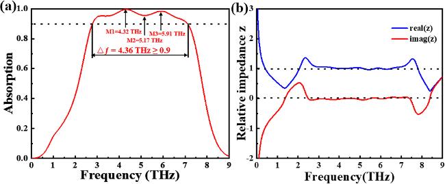
Figure 2. The absorption spectrum of the absorber from 0 to 9 THz (a); Real and imaginary components of the relative impedance z of the absorber (b). |
We compared the absorber with other published papers in terms of the number of structural layers and absorption performance, as shown the table 1 [37-41]. The biggest advantage of our absorber is that the graphene model has only a simple three-layer structure and can achieve a wider bandwidth at terahertz frequencies, which is wider than other papers.
Table 1. The absorption bandwidth and the number of structural layers of the proposed absorber are compared with previous absorbers. |
To investigate the absorption characteristics of this structure deeply, this study applied impedance matching theory [42-44], the relative impedance refers to the difference between the characteristic impedance of the material and the impedance of the free space. In the transmission line theory, when the impedance of the incident electromagnetic wave matches the characteristic impedance of the material, the energy of the electromagnetic wave will enter the material as much as possible, reducing the reflection and increasing the absorption, the relative impedance is expressed by equation (5 )
$\begin{eqnarray}{\rm{Z}}={\rm{\pm }}\sqrt{\frac{{\left(1+{S}_{11}\right)}^{2}-{{S}_{21}}^{2}}{{\left(1-{S}_{11}\right)}^{2}-{{S}_{21}}^{2}}},\end{eqnarray}$
As shown in figure 2(b), after careful analysis, it was found that in the frequency range of 2.78 to 7.14 THz, the real part of the complex impedance of the absorber is almost equal to 1 [45], while its imaginary part remains roughly at 0. This result indicates that the absorber satisfies the relative impedance matching theory, the reflectivity of the frequency band is greatly reduced, and the absorber obtains excellent absorption performance [46,47]. This also confirms the simulation results of the absorber in figure 2(a), which shows almost perfect absorption in the 2.78-7.14 THz band.
We investigated the absorption performance of the absorber being irradiated at different angles of polarization and irradiation. As shown in figure 3(a), the absorption spectra at various incidence angles under transverse magnetic (TM) wave state are presented, while figure 3(b) shows the absorption spectra at different incidence angles under TM wave state. Through analysis, it was found that the change in polarization angle has exert minimal influence on absorbance, which is because the graphene layer pattern of our absorber model is centrosymmetric. This feature enables it to provide consistent performance in different polarization states, making it flexible to be applied in practice [48,49]. At the same time, according to figures 3(a) and (b), it is found that in TE mode, excellent broadband absorption performance can be achieved within the incident angle range of 0° to 30°. Specifically, when the light is incident at a 20° angle, the absorption efficiency at the M2 position can reach 93.2%, the average absorption rate is about 96%, and the absorption efficiency gradually decreases with increasing incident angle. However, in the range of 0∼50° incidence angles, the absorption rate can always be maintained above 90%. In TM mode, the absorber can also maintain good broadband absorption in the range of 0°∼50°, the absorption rate is always greater than 90%. This indicates that the absorbent material has angular incident insensitivity. In the frequency range of 2.78-6.14 THz, the average absorption of the absorber at the incidence angles of 0°∼50° is 91.7% (TE) and 94% (TM). Therefore, in the TM mode, our absorber is more insensitive to the incidence angle. This is because in TM mode, the surface plasmon resonance effect exhibited by the absorbing material significantly enhances its light absorption ability, the local surface plasmon resonance is a phenomenon of collective oscillation of free electrons on the metal surface. When the frequency of the incident wave matches the collective oscillation frequency of free electrons on the metal surface, the resonance can significantly improve the absorption rate of the structure [50,51].
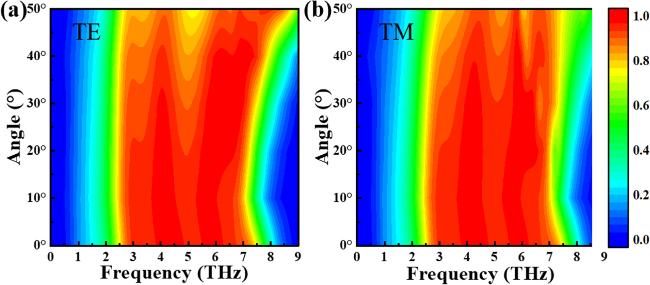
Figure 3. Absorption spectra of absorbing materials in TE mode (a). Absorption Spectra of absorbing materials in TM mode (b). |
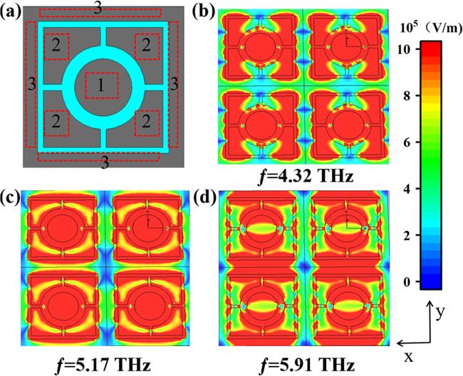
Figure 4. The unit surface of the absorber (a). Electric field distribution at three frequency points f=4.32 THz(b), f=5.17 THz(c), f=5.91 THz(d) for normal incident. |
Figure 4(a) depicts three regions of the graphene layer, figures 4(b)-(d) describes the electric field distribution of the absorber at three frequency points. The collective resonance composed of the above three regions successfully revealed the mechanism of broadband absorption. We further studied the contribution of a single region and the combination of two regions to broadband absorption. figure 5 presents the absorption spectral lines of a specific region and the electric field distribution of three different modes M1, M2, and M3. By analyzing parts (a), (e), and (i) of figure 5, it can be observed that region 1 exhibits a significant absorption peak at a frequency of 5.17 THz, with an absorption efficiency of approximately 83%. Region 2 exhibits a higher absorption peak at a frequency of 3.27 THz, with an efficiency of 93.3%, and forms a wider absorption band in the mid-frequency range, Region 3 exhibits its absorption peak at 7.14 THz. These three regions have made significant contributions to improving absorption within their specific frequency ranges. Further observation of parts (b) to (d) of figure 5 reveals that region 1 exhibits the most significant plasma resonance phenomenon [52,53] at a frequency of 5.17 THz, resulting in a concentrated distribution of electric fields and a higher absorption rate at this frequency. Through figures 5(f)-(h), we can see that region 2 has relatively strong plasmon resonance in the mid-frequency band, which reveals the contribution of region 2 to the bandwidth absorbed by the broadband. As shown in figures 5(j)-(l), the surface plasmon resonance [54-56] of region 3 is gradually enhanced with the increase of frequency, which reveals the contribution of Region 3 to the absorption rate of high frequency band.
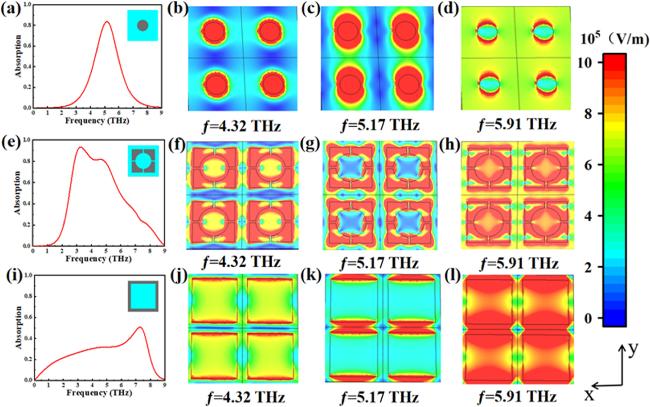
Figure 5. The absorption curve of region 1 and the electric field distribution at three frequency points f=4.32 THz(b), f=5.17 THz(c), f=5.91 THz(d) at normal incidence. The absorption curve of region 2 and the electric field distribution at three frequency points f=4.32 THz(f), f=5.17 THz(g), f=5.91 THz(h) at normal incidence. The absorption curve of region 3 and the electric field distribution at three frequency points, f=4.32 THz(j), f=5.17 THz(k), f=5.91 THz(l) at normal incidence. |
After discussing the contribution of a single region to the absorber, we then proceed to investigate the contribution of the combination of two regions to the absorption. From figures 6(a), (e), and (i), we can see that the absorption rate of region 12 in the range of 3.06-5.77 (2.11) THz exceeds 90%, the highest absorption rate is 99.7% at 4.74 THz. Region 13 has the highest absorption at 5.17 THz with an absorption rate of about 95.7%. The absorption rate of region 23 is more than 80% in 2.58-7.32 (4.74) THz, so we can conclude that the region 12 combination contributes to the absorption rate of the middle band, the region 13 combination contributes to the absorption rate, and the region 23 combination contributes to the bandwidth, and the three regions are combined together to obtain good absorption performance with high absorption rate and wideband. By observing figures 6(b)-(d) and (f)-(h), we find that the surface plasmon resonance of region 12 combination and region 13 combination at 5.17 THz shows a strong intensity, this results in a highly concentrated electric field distribution in the region, causing the absorption efficiency of electromagnetic wave energy projected onto it to reach its peak [57]. From figures 6(j)-(l), we find that the electric field of combination region 23 is densely distributed at 5.91 THz, which indicates that this combination region contributes to the absorption rate of high frequency bands. In short, the strong electric fields in different regions are coupled with each other, which leads to the formation of the absorption broadband [58].
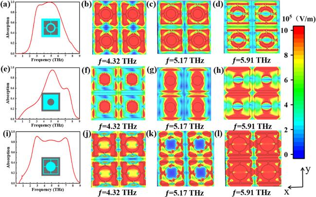
Figure 6. The absorption spectrum region 12 (a) and their electric field distributions at 4.32 THz(b), 5.17 THz(c), 5.91 THz(d). The absorption spectrum region 13(e) and their electric field distributions at 4.32 THz(f), 5.17 THz(g), 5.91 THz(h). The absorption spectrum region 23 (i) and their electric field distributions at 4.32 THz(j), 5.17 THz(k), 5.91 THz(l). |
The adjustment of the period length of the dielectric layer and the unit structure is conducive to improving the performance of the absorber. As shown in figure 7(a), the absorption spectrum shows a redshift trend with H2 increases from 11 μm to 15 μm, this is because the thicker dielectric layer effectively changes the propagation conditions of the surface plasma mode, resulting in lower energy photons being able to excite the surface plasma, thus making the absorbed spectrum shift towards longer wavelengths, its absorption efficiency keeps exceeding 90%. Specifically, at a thickness of 13 μm, the frequency bandwidth with an absorption efficiency exceeding 90% is 4.36 THz, while at a thickness of 14 μm, this width is reduced to 3.55 THz. This change further confirms the core role of H2 in absorbing materials. From the analysis of figure 7(b), it is evident that when the period length reaches 27 μm, the absorption frequency band achieves its maximum width. With an increase or decrease in P, the overall absorption bandwidth shows a narrowing trend. When P=26 μm, the absorption bandwidth is 3.66 THz, indicating that P could affect the local surface plasmonal resonance of the high frequency part, thus affecting the absorption bandwidth of the absorber [59,60]. We can adjust the relevant parameters according to the actual application.
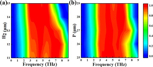
Figure 7. Absorption spectra at varying H2 conditions (a). Absorption spectra at varying P conditions (b). |
After that, we also studied the influence of key parameters of the separation structure on the overall absorption performance. As seen in figure 8(a), the absorption spectrum as a whole shows a redshift trend as W1 increases from 0.2 μm to 1.0 μm. When W1=1 μm, the highest absorption rate (99.7%) is reached at M1 (4.32 THz), and the widest absorption bandwidth (4.36 THz) is reached. According to figure 8(b), the absorption rate of W2 from 12 μm to 16 μm is always above 90%, and the absorption bandwidth presents a trend of first narrowing and then widening. The bandwidth is 1.87 THz at 12 μm, and the widest absorption band is 4.36 THz when W2 is 14 μm. Similarly, as seen in figure 8(c), the absorption rate is not reduced. The absorber has the widest absorption band when W3 is 4.8 μm. Looking at figure 8(d), when L2 gradually increases from 17 μm, we find that the absorption bandwidth becomes narrower. The results show that the L2 has a significant effect on the width of the absorption bandwidth. Through comprehensive analysis, the physical characteristics of the separated structure will have a decisive impact on the bandwidth and absorption frequency range of the absorber. By adjusting these parameters, the absorber can be tunable, so that it can be flexibly applied to detection, modulation and other scenarios.
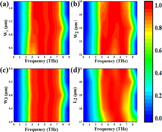
Figure 8. Effects of key parameters of separation structure on the absorption efficiency. Effects of w1 (a), effects of w2 (b), effects of w3 (c), effects of L2 (d). |
The absorber proposed in this article was compared and analyzed in detail with other similar structural models shown in table 2 [61-63]. Amirhossein proposed three-layer metamaterial absorber has a bandwidth of 2.173 (1.482-3.655) THz, Pouria et al designed a terahertz multilayer metamaterial perfect absorber with a perfect absorption narrow band at 2.6 THz and 4.8 THz, the absorber structure designed by Peiman et al has excellent absorption of 99.99% at 7.628 THz, but lacks tunability, so our advantage is that we have wider absorption bandwidth and tunability.
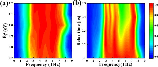
Based on the excellent tunability of Fermi levels in graphene, we investigated how changes in the Fermi level affect the absorption properties of graphene layers by applying an external voltage to control it. figure 9(a) illustrates the light absorption efficiency of the absorbing material at various Fermi energy levels. Obviously, as the Fermi energy increases from 0.7 eV to 1.0 eV, the absorption bandwidth gradually increases, at 0.7 eV, the absorption bandwidth is 3.19 THz (3.48-6.67 THz), and at 1.0 eV, the absorption bandwidth is 4.36 THz (2.78-7.14 THz). This makes it possible to obtain the required absorption frequency band by adjusting the tuned Fermi energy under different scene requirements. With increasing chemical potential, absorption efficiency rises, at the Fermi energy of 0.7 eV, the average absorption rate is about 87%, while at 1.0 eV it is about 96%. This is related to the concentration of charge carriers in graphene, when the incident light comes into contact with the charge carriers inside graphene, these charge carriers collectively undergo resonant reactions, which are closely connected to the density of charge carriers, and the density of charge carriers is directly affected by the Fermi energy Ef of graphene. Fermi energy [64,65] is expressed by equation (6 )
$\begin{eqnarray}{E}_{{\rm{f}}}={\rm{ \hbar }}{\nu }_{{\rm{f}}}{\left(\pi N\right)}^{1/2}.\end{eqnarray}$
Figure 9. Effect of Fermi energy on absorption rate (a). Effect of relaxation time on absorption rate (b). |
In the process of adjusting the carrier concentration N, it can be achieved by chemical doping. The increase of Fermi level leads to the increase of carrier concentration and the increase of collective carrier oscillation, which decreases the damping coefficient. Thus, the absorption peak is produced.
We also explored the impact of various relaxation times, which can be achieved by adjusting carrier mobility, the relaxation time τ can be expressed as τ=$\frac{{\mu E}_{{\rm{f}}}}{{{{\rm{e}}\nu }_{{\rm{f}}}}^{2}}$. Therefore, by adjusting the migration efficiency of charge carriers or chemical doping methods, the relaxation time can be adjusted. Graphene generally has a relatively short relaxation time due to its rapid response to photons [66,67]. As shown in figure 9(b), when we adjust the relaxation time to 1 ps, the absorption performance is good, as the relaxation time increases, the absorption band gradually moves from wideband to narrow band, which is advantageous to obtain a narrow band absorber. Narrow-band absorbers are of great significance in the fields of narrow-band thermal radiation, photoelectric detection and biosensing [59]. The reason why the absorption bandwidth of the absorber is widest when τ=0.1 ps is the carrier participating in plasma oscillation absorption reaches saturation. If the relaxation time is extended, the reflected energy will increase, resulting in a decrease in the absorption bandwidth [60].
4. Conclusion
In short, we propose a broadband tunable metamaterial absorber using graphene. The simulation results using CST software indicate that the absorption rate exceeds 90% between 2.78 and 7.14 (4.36) THz, while it reaches over 99% from 4.1 to 4.54 (0.44) THz. The absorption meets the impedance matching theory. The wideband absorption mechanism is revealed by studying the surface electric field intensity distribution of the absorber unit structure, its separation structure, and the combined structure in different regions. By studying the influence of small changes in dielectric layer thickness, the unit period length, the separation structure and other geometric parameters, it is found that the absorption frequency band and bandwidth are tunable. In addition, adjusting the bias voltage and transforming the chemical potential energy can regulate the absorption spectral bands. After studying the absorption performance under various polarization states and incidence angles, it was observed that the absorber exhibits insensitivity to changes in polarization direction and wide-angle incidence. On this basis, the mechanism of how relaxation time affects absorption performance was explained using the carrier theory of plasma vibration. In summary, we designed a tunable metamaterial absorber with simple structure, high absorption rate and wide absorption band, which has many characteristics and has broad application significance in the field of terahertz band absorber.
Acknowledgments
The authors are grateful to the support form the National Natural Science Foundation of China (Grant Nos. 51606158, 11604311, 12074151), the Funded by the Guangxi Science and Technology Base and Talent Special Project (Grant No. AD21075009), the funded by the Sichuan Science and Technology Program (Grant No. 2021JDRC0022), the Open Fund of the Key Laboratory for Metallurgical Equipment and Control Technology of Ministry of Education in Wuhan University of Science and Technology, China (Grant Nos. MECOF2022B01; MECOF2023B04); the Project supported by Guangxi Key Laboratory of Precision Navigation Technology and Application, Guilin University of Electronic Technology (Grant No. DH202321).
Competing financial interests
The authors declare no competing financial interests.