


1. Introduction
Flexible electronics technology has demonstrated revolutionary application potential in fields such as wearable health monitors [1, 2], foldable displays [3], and implantable medical devices [4, 5]. Graphene, a two-dimensional material composed of a single layer of carbon atoms arranged in a hexagonal honeycomb lattice, combines structural flexibility with exceptional mechanical properties [6–9]. These attributes, together with ultra-thin and lightweight characteristics, render graphene an ideal candidate for flexible electronic devices [10, 11]. It possesses an extraordinary elastic modulus of 1 TPa and an ideal tensile strength of 100 − 130 GPa [9, 12]. Such mechanical properties enable graphene to withstand various forms of strain, including bending [13–18], twisting [19–21], and bubbling [22, 23].
The unique electronic properties of graphene are particularly noteworthy [24]. Its linear dispersion relation near the K/$K^{\prime} $ points in the Brillouin zone forms a double Dirac cone structure. Notably, elastic strain can effectively modulate the electronic band structure of graphene [25–29]. Lattice distortion modifies electron hopping integrals, generating an effective gauge field acting on the electron-hole system. This gauge field can induce pseudo-magnetic fields exceeding hundreds of Teslas and create pseudo-Landau quantization levels near the Dirac cones. Guinea et al have theoretically demonstrated that strain configurations with triangular symmetry can produce uniform pseudo-magnetic fields in graphene [30]. Iva et al have observed pseudo-Landau levels in graphene via scanning tunneling microscopy (STM) by engineering a periodically strained superlattice induced by a hexagonal array of silica nanospheres [31]. Levy et al have experimentally confirmed that localized strain in graphene nanobubbles generates pseudo-magnetic fields surpassing 300 T, where pseudo-Landau levels were observed through scanning tunneling spectroscopy [32].
In crystals, the band extrema near specific high-symmetry points in momentum space are referred to as valleys [33, 34]. The two inequivalent Dirac points at the charge neutrality point endow graphene with a novel degree of freedom analogous to spin. To utilize valleys as practical information carriers, it becomes crucial to distinguish and control valley polarization. Considerable efforts have been devoted to exploring valley-filtering effects in bulk graphene systems. Garcia-Pomar et al have achieved the splitting and collimation of fully valley-polarized electron beams through interface engineering of n-p–n junctions, leveraging the triangular warping effect of valleys [35]. Yin et al have directly probed the tunable valley-selective Hall effect in bilayer graphene with variable bandgap by valley-polarizing carriers with circularly polarized infrared light [36]. A gate-tunable valley filter has been put forward based on strained graphene and local magnetic modulation [37]. Sharma et al have demonstrated theoretically that in minimally gapped graphene, high-purity valley-polarized currents can be induced by double-pumped terahertz light combining circularly polarized and linearly polarized components [38]. Song et al have theoretically demonstrated a fully valley-polarized currents in strained graphene under periodic magnetic field modulation [16]. Li et al have experimentally achieved valley polarization and controllable valley inversion in graphene through the combined effects of strain-induced pseudomagnetic fields and real magnetic fields [26]. Notably, Settnes et al have revealed a pseudomagnetic field-induced real-space valley separation mechanism in graphene nanobubbles with Gaussian profiles, proposing a novel approach for field-free valley manipulation [39].
The fabrication of one-dimensional graphene nanoribbons along specific crystallographic directions produces two types of edge terminations, zigzag and armchair nanoribbons, with fundamentally different electronic characteristics [40]. In graphene nanoribbons with armchair edges, topological phase transition induced by strain or light has been predicted recently [41, 42]. However, for armchair-edged graphene nanoribbons one cannot define the valley points. In zigzag graphene nanoribbons (ZGNRs), the energy spectrum hosts not only two completely separated valleys (K/$K^{\prime} $) but also a metallic quasi-flat band due to edge-localized states [43, 44]. These unique properties make ZGNRs an ideal platform for valley-related phenomena. Rycerz et al have proposed to implement valley filter and valve functionalities using quantum point contact structures based on zigzag edges [45]. Through theoretical modeling, Kundu et al have demonstrated highly valley-selective transport in ZGNRs under the shine of a circularly polarized light and its fourth harmonic [46]. Furthermore, strain engineering provides an alternative pathway for valley manipulation without external fields. Hurtubise et al have demonstrated that applying uniaxial strain patterns in ZGNRs enables pure valley currents [25]. Zhang et al have quantitatively revealed strain-induced pseudomagnetic fields in twisted graphene nanoribbons, leading to valley-polarized edge and central serpentine orbital currents [47].
Among various strain forms, in-plane bending strain combines reversibility with precise controllability. Lit et al have achieved precise control of in-plane bending in armchair-shaped nanoribbons using scanning tunneling microscopy (STM) [48]. Inspired by this advance, in this work we explore the effect of flexibility on conductance and valley polarization in ZGNRs. In the considered device, a rectangular portion of ZGNR is bent into an arc with angle φ. Based on a tight-binding model with distance-dependent hopping energies, we find that the pseudo-Landau levels in the bent region become progressively more pronounced with the increasing of bending angle φ. Accordingly, the bending deformation enlarges the plateau of full valley polarization near the Dirac points. When the positive Fermi energy approaches the bottom of a pseudo-Landau level n from below, Fano antiresonance appears in the valley-resolved conductance, which is due to the interference between the propagating mode in the (n − 1)th pseudo-Landau level and evanescent mode derived from the nth pseudo-Landau level. At φ = 180∘, the transmission drop at the conductance dips can exceed 0.8. At these valley-resolved conductance dips, remarkable valley polarization (with amplitude exceeding 70%) can be obtained.
2. Model and formula
The considered device is illustrated in figure 1, which is initially a ZGNR of width W in the (x, y) plane [figure 1(a)]. An in-plane bending strain is applied to the central region of length L, transforming the original rectangular structure into a circular arc [figure 1(b)]. The arc is characterized by the bending radius R and central angle φ = L/R. The lead regions remain unstrained and are seamlessly connected along the tangential directions at both ends of the bent central region. Within the nearest-neighbor tight-binding approximation, the Hamiltonian is expressed as
$\begin{eqnarray}H=\displaystyle \sum _{{\boldsymbol{r}},i}{t}_{i}{b}_{{\boldsymbol{r}}+{{\boldsymbol{\alpha }}}_{{\boldsymbol{i}}}}^{\dagger }{a}_{{\boldsymbol{r}}}+\,\rm{H.c.}\,,\end{eqnarray}$
where ar and ${b}_{{\boldsymbol{r}}+{{\boldsymbol{\alpha }}}_{{\boldsymbol{i}}}}^{\dagger }$ denote annihilation and creation operators for electrons on the sublattice A and B, respectively. The nearest-neighbor vectors αi [shown in the inset of figure 1(a)] are explicitly defined as $\begin{eqnarray}{{\boldsymbol{\alpha }}}_{1}={a}_{0}\left(0,-1\right),\end{eqnarray}$
$\begin{eqnarray}{{\boldsymbol{\alpha }}}_{2}={a}_{0}\left(-\frac{\sqrt{3}}{2},\frac{1}{2}\right),\end{eqnarray}$
$\begin{eqnarray}{{\boldsymbol{\alpha }}}_{3}={a}_{0}\left(\frac{\sqrt{3}}{2},\frac{1}{2}\right).\end{eqnarray}$
These vectors have the same magnitude ∣αi∣ = a0 = 0.142 nm (corresponding to the carbon-carbon bond length). The hopping integrals ti are modulated by strain, $\begin{eqnarray}{t}_{i}=t\exp \left[-g\left(\frac{\left|{{\boldsymbol{\alpha }}}_{i}+{\boldsymbol{u}}({\boldsymbol{r}}+{{\boldsymbol{\alpha }}}_{i})-{\boldsymbol{u}}({\boldsymbol{r}})\right|}{{a}_{0}}-1\right)\right].\end{eqnarray}$
Here the unstrained hopping integral is t = −2.8 eV, ur describes the lattice displacement at position r, and the parameter g = 3.37 governs the spatial decay rate of hopping energy with bond length [49]. Note that ur = 0 in the lead regions.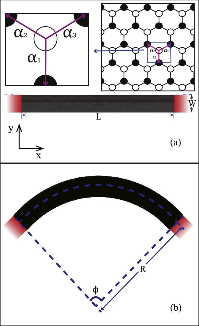
Figure 1. Schematic illustration of the considered ZGNR device in the (x, y) plane. (a) Unstrained configuration: the nanoribbon has width W. The central scattering region (black area) has length L. Inset shows the hexagonal lattice structure with three nearest-neighbor vectors α1, α2, and α3. (b) Strained configuration: In-plane bending strain is applied to the central region, forming an arc with curvature radius R and central angle φ = L/R. |
In the ZGNR leads, the K and $K^{\prime} $ valleys are located at 2π/(3a) and −2π/(3a), respectively, where the lattice constant a = 0.246 nm. The band structure En(k) for the width W = 20 nm is plotted in figure 2(a). The positive direction of the wave vector k is taken to point towards infinity rather than the central region. For a propagating mode with wave vector k in the subband n, its traveling direction is determined by the group velocity vn(k) = ∂ℏkEn(k), while its valley index is assigned by the distance ∣k − K∣ and $| k-K^{\prime} | $. If 0 < k < π/a (−π/a < k < 0), it is categorized [45] as belonging to the K ($K^{\prime} $) valley. Note that the ingoing/outgoing modes in the leads have negative/positive group velocity. In either lead, the number of ingoing modes, denoted as N(E), equals that of outgoing modes.
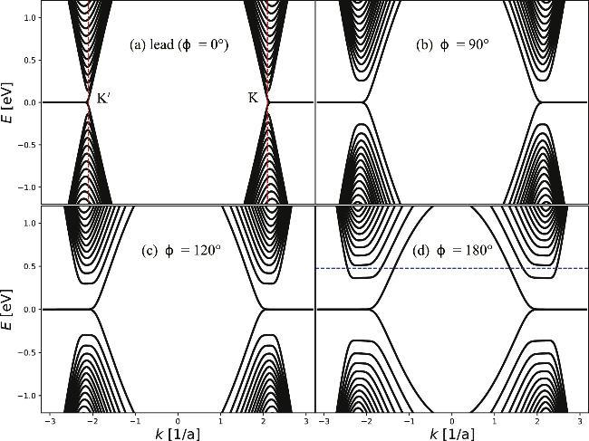
Figure 2. Energy bands of the lead (a) and the bent region with different bending angles φ = 90∘ (b), 120∘ (c), and 180∘ (d). The vertical (red dashed) lines in (a) indicate the positions of the K and $K^{\prime} $ valleys. The horizontal (blue dashed) line in (d) with energy 0.477 eV corresponds to a Fano resonance in figure 3(a). |
The transport problem prescribed by equations (1 ) and (5 ) can be constructed and then solved by the Kwant package [50]. Particularly, we yield numerically the transmission probability Tp,q(E) for an electron with energy E scattering from the mode q in the left lead to the mode p in the right lead [1 ≤ p, q ≤ N(E)]. At the Fermi energy EF and under zero temperature, the valley-resolved conductance Gμ ($\mu \in \{K,K^{\prime} \}$) of the considered device is given by the Landauer–Büttiker formula [51, 52],
$\begin{eqnarray}{G}_{\mu }({E}_{F})=\frac{2{e}^{2}}{h}\displaystyle \sum _{p=1}^{N({E}_{F})}\displaystyle \sum _{q=1}^{N({E}_{F})}{T}_{p,q}({E}_{F}){V}_{\mu ,p}({E}_{F}),\end{eqnarray}$
where e represents the elementary charge, h is the Planck constant, and the valley indicator Vμ,p is set at 1 when the outgoing mode p belongs to the μ valley and 0 otherwise.The valley polarization of the output current is defined as
$\begin{eqnarray}P({E}_{F})=\frac{{G}_{K\,}({E}_{F})-{G}_{K^{\prime} }({E}_{F})}{{G}_{K}({E}_{F})+{G}_{K^{\prime} }({E}_{F})}.\end{eqnarray}$
The valley polarization P lies in [−1, 1], where P = ±1 corresponds to complete K/$K^{\prime} $ valley polarization (exclusively K/$K^{\prime} $ valley transport), and P = 0 represents no valley selectivity.3. Results and discussions
3.1. Pseudo-Landau levels in the bent region
Under in-plane bending deformation [figure 1(b)], the central arc length of the nanoribbon is equal to the original length L, while the width W is preserved. Under this geometric constraint, the tangential projection of the chemical bonds shows a linear variation with the position coordinate of the sites, while the radial projection remains unchanged [49, 53]. In the bent region the three nearest-neighbor vectors ${\boldsymbol{\alpha }}{{\prime} }_{1}$, ${\boldsymbol{\alpha }}{{\prime} }_{2}$ and ${\boldsymbol{\alpha }}{{\prime} }_{2}$ can be expressed as 5 ), the strain-modulated hopping integrals ti become 1 ) can be transformed into a portion of a one-dimensional (1D) periodic model. For such a 1D chain, the application of Bloch theorem (or Fourier transform) leads to a matrix Hk with dimension 2N, where N is the number of dimers along the y-direction of the undeformed nanoribbon, and k is the Bloch wave vector. Then the energy band structure in the bent region can be obtained through numerical diagonalization of Hk.
$\begin{eqnarray}{\boldsymbol{\alpha }}{{\prime} }_{1}={a}_{0}\left(0,-1\right),\end{eqnarray}$
$\begin{eqnarray}{\boldsymbol{\alpha }}{{\prime} }_{2}={a}_{0}\left(-\frac{\sqrt{3}}{2}\left(1+\frac{y}{R}\right),\frac{1}{2}\right),\end{eqnarray}$
$\begin{eqnarray}{\boldsymbol{\alpha }}{{\prime} }_{3}={a}_{0}\left(\frac{\sqrt{3}}{2}\left(1+\frac{y}{R}\right),\frac{1}{2}\right),\end{eqnarray}$
where y ∈ [−W/2, W/2] denotes the y coordinate of original lattice sites. According to equation ( $\begin{eqnarray}{t}_{1}=t,\end{eqnarray}$
$\begin{eqnarray}{t}_{2,3}=t\exp \left[-g\left(\sqrt{\frac{3}{4}{\left(1+\frac{1}{R}y\right)}^{2}+\left(\frac{1}{4}\right)}-1\right)\right].\end{eqnarray}$
Note that these hopping integrals are independent of the x coordinate. In the bent region, the tight-binding Hamiltonian in equation (In figure 2, we plot the energy spectra En(k) for the strain-free lead region (corresponding to φ = 0∘) and bent region with φ = 90∘, 120∘, and 180∘. The width of the ZGNR is set at W = 20 nm, while the central region has original length L = 200 nm. Both molecular dynamics simulation [54] and STM manipulation [48] have confirmed that when the width of graphene nanoribbons exceeds 1.5 nm, stable bending occurs for curvatures below 2 deg/nm. For the largest bending angle φ = 180∘ under consideration, the curvature is κ = φ/L = 0.9 deg/nm, which falls well within the experimentally accessible regime. In addition, for maintaining the structural integrity, the dimensionless parameter Θ = W/(2R) should be smaller than 0.2 [53]. At φ = 180∘, Θ ≈ 0.157 is indeed below the threshold. The dispersion relations satisfy En(k) = En(−k) and exhibit particle-hole symmetry. In the lead region, there exist a series of conduction/valence subbands with minimum/maximum near the K or $K^{\prime} $ point. These subbands can be identified by the band index n and valley index μ. The conduction subband with index n = 0, 1, 2, 3,… has minimum En,c, while the valence subband with index n = −1, −2, −3,… has maximum En,v. Here E−m,v = −Em−1,c decreases with the positive integer m. The lowest conduction subband (with n = 0 and E0,c = 0) is connected to the zero-energy quasi-flat band at the K ($K^{\prime} $) point, whose velocity is always negative (positive). The valley-dependent propagating direction of this mode is crucial for valley filtering in several ZGNR-based devices [45]. In the bent region, it can be seen that the bottom En,c(φ) of conduction subbands with index n > 0 moves up with the increasing of bending angle φ. The n = 0 conduction subbands still start from the zero-energy. Several lowest-lying conduction subbands (n ≤ 4 for φ = 180∘) have a nearly flat bottom, indicating the formation of pseudo-Landau levels. For these subbands in the K ($K^{\prime} $) valley, the amplitude of velocity at the left (right) of the flat bottom is lower than that in the lead region. The velocity mismatching and pseudo-Landau levels becomes more and more pronounced as φ increases. These features induced by the bending deformation can be understood from the analytical model in [49, 53], which will be used to analyze valley-polarized transport in the device shown in figure 1(b).
3.2. Effect of bending strain on valley-resolved conductance and valley polarization
For the ZGNR-based device, we calculate numerically the valley-resolved conductance GK [figure 3(a)] and ${G}_{K^{\prime} }$ [figure 3(b)] as well as valley polarization P (figure 4) as functions of the Fermi energy EF. The size parameters are the same as in figure 2, while the in-plane bending angle φ is set at 0∘ (no bending), 30∘, 90∘, 120∘, and 180∘. The conductance spectrum GK is related to ${G}_{K^{\prime} }$ by a mirror symmetry about zero energy, i.e., ${G}_{K}({E}_{F})={G}_{K^{\prime} }(-{E}_{F})$. This relation originates from the particle-hole symmetry in the considered tight-binding model. We thus focus our discussion on the K valley.
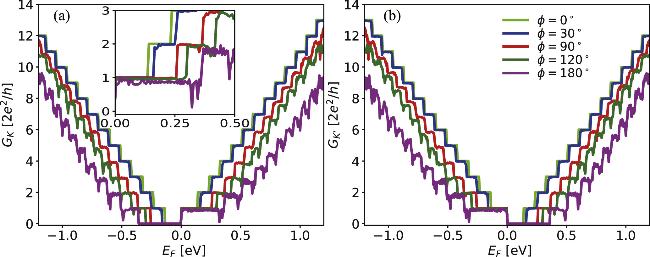
Figure 3. Valley-resolved conductance Gμ under different bending angles φ plotted as a function of Fermi energy EF. (a) μ = K; (b) μ = $K^{\prime} $. The inset in (a) shows the zoom-in image of K valley conductance within the energy window $\left(0,0.5\right)$ eV. The solid curves in fluorescent green, blue, red, dark green, and purple are respectively for φ = 0∘ (no bending), 30∘, 90∘, 120∘, and 180∘. |
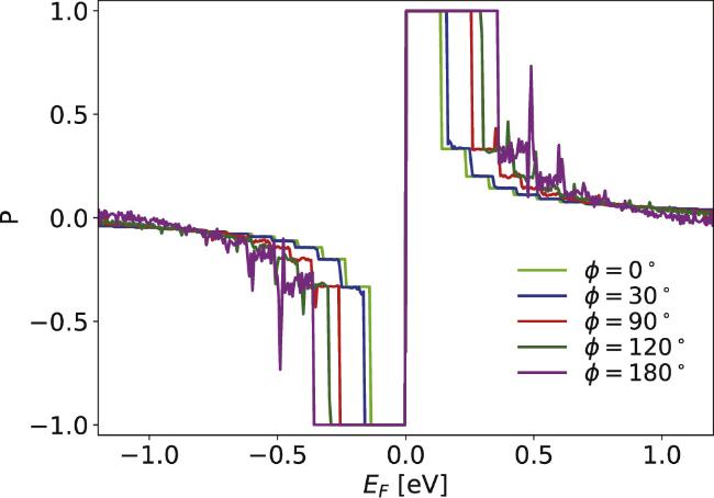
Figure 4. Valley polarization P as a function of Fermi energy EF. All other parameters are the same as in figure 3. |
In the strain-free case (φ = 0∘), the conductance GK plotted in figure 3(a) exhibits distinct quantized steps, which is determined by the number N(EF, K) of outgoing modes in the K valley of the right lead, i.e., GK = N(EF, K)G0 with G0 = 2e2/h. We can write
$\begin{eqnarray}N\left({E}_{F},K\right)=\left({n}_{1}+1\right){\rm{\Theta }}\left({E}_{F}\right)+{n}_{2}{\rm{\Theta }}\left(-{E}_{F}\right),\end{eqnarray}$
where the integer n1 and n2 are nonnegative, and Θ(x) is the Heaviside step function. For EF > 0, the subband ${E}_{{n}_{1}+1}(k)$ in figure 2(a) is the first conduction subband globally above EF. When EF < 0, the subband ${E}_{-{n}_{2}-1}(k)$ is the last valence subband crossing the line E = EF. The width of conductance plateau equals the energy spacing between the minimum ${E}_{{n}_{1},c}$ and ${E}_{{n}_{1}+1,c}$ (maximum ${E}_{-{n}_{2},v}$ and ${E}_{-{n}_{2}-1,v}$) of two adjacent conductance (valence) subbands. In the case E−2,v < EF < 0 (E−2,v = −0.137 eV for W = 20 nm), one has GK = 0 and ${G}_{K^{\prime} }={G}_{0}$, indicating a unidirectional transport channel contributed from a single valley. The reason is that edge states from different valleys propagate in opposite directions [see figure 2(a)].With the increasing of the bending angle φ, the valley conductance GK moves down globally [figure 3(a)]. The reason is that in the bent region En,c(φ) and ∣E−n,v(φ)∣ with n > 0 increase with φ, which leads to the reduction in the number of available propagating states with energy EF in the bent region. Since the conductance spectrum at φ > 0 exhibits a similar step-like trend as the case φ = 0, we can still use the integer n1 and n2 in equation (13 ) to label the conductance plateaus. Notably, both the transmission-forbidden region (n2 = 0) and single-channel transport regime (n1 = 0) expand remarkably as φ increases, which are determined by E1,c(φ). As shown in the inset of figure 3(a), the conductance plateau with n1 = 0 is not flat, which shows small and rapid oscillations at φ = 180∘. These oscillations result from the velocity mismatching of edge states between the lead and the bent region.
For φ ≤ 90∘, the conductance plateaus of GK are relatively complete. For φ ≥ 120∘, the transition regions of adjacent conductance steps become wide. Accordingly, the conductance plateaus for n1 > 1 or n2 > 1 shrink. In addition, one can observe conductance dips before the onset of new steps. As illustrated in the inset of figure 3(a), at bending angle φ = 180∘ a distinct asymmetric antiresonance emerges in the conductance spectrum with energy 0.477 eV. The transmission drop at this conductance dip exceeds 0.955. Such pronounced conductance dips originates from the Fano resonance effect of electrons [55, 56]. As shown in figure 2(d), an electron incident with energy E = 0.477 eV can traverse the bent region via either the propagate mode in the subband E1,K or the bound state derived from the pesudo-Landau level in the subband E2,K. The interference between the two waves (described by the propagate mode and bound state) triggers the Fano-type anti-resonance phenomenon. Thus the conductance dips in figure 3 can be attributed to the subband interaction, where the pesudo-Landau levels provide the bound states.
In figure 4 we plot the valley polarization P under several values of bending angle φ. It can be seen that P is antisymmetric about EF = 0, i.e., P(EF) = −P( − EF), which results from the symmetry ${G}_{K}({E}_{F})={G}_{K^{\prime} }(-{E}_{F})$ demonstrated in figure 3. Consequently, the valley polarization is reversed at EF = 0. In the case φ = 0∘ and EF > 0, when the K-valley conductance reaches plateaus GK = (n1 + 1)G0 (n1 = 0, 1, 2…), one has ${G}_{{K}^{{\prime} }}={n}_{1}{G}_{0}$ and thus valley polarization [45] P = 1/(2n1 + 1). As EF increases from 0 to 1.2 eV, P decreases from 100% to 4%. The bending strain alters significantly the magnitude of valley polarization. On the plateau n1 = 0 of GK, one yields a full valley polarization (P = +1). The full polarization plateau broadens progressively from 0.135 eV at φ = 0∘ to 0.357 eV at φ = 180∘. In the energy range 0.135 eV < EF < 0.795 eV, the valley polarization is basically enhanced by increasing φ. Near the Fano antiresonances of GK (${G}_{K^{\prime} }$), the valley polarization drops (raises) abruptly. At φ = 180∘, the Fano anti-resonance of ${G}_{K^{\prime} }$ at EF = 0.489 eV leads to a valley polarization P = 73%, which is much larger than the corresponding value (11%) in the unstrained case. In contrast, the conductance dip of GK at EF = 0.477 eV results in a drastic drop of valley polarization (<11%). At EF = 1.2 eV, the valley polarization changes its sign (P = −3.6%) at φ = 180∘.
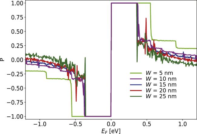
Finally, we explore the influence of ZGNR width W on the strain-induced valley polarization P. The original length of the central region and the bending angle are fixed at L = 200 nm and φ = 180∘. In figure 5, we plot the variation of P with EF for the width W = 5, 10, 15, 20, and 25 nm. For a narrow ZGNR such as W = 5 nm, the valley polarization minorly deviates from the plateaus (±1, ±1/3, ±1/5,…) obtained in the strain-free case. The full valley polarization plateau P = +1 (with width 0.55 eV) is obviously wider than that (0.357 eV) under W = 25 nm. From the energy spectra (not shown here) we find that pseudo-Landau levels are absent at W = 5 nm and appear at W ≥ 10 nm. For the first pseudo-Landau level, E1,c in the large W limit depends only on the curvature 1/R [see equation (19) of [49]]. Accordingly, the valley polarization plateau P = +1 is almost the same for all width W ≥ 10 nm. Note that its strain-free counterpart decreases quickly with the width W. As the width W increases from 10 nm, the valley polarization P in the energy range 0.369 eV < EF < 0.88 eV decreases globally and deviates seriously from the step-like features. One can clearly see the inversion of valley polarization for the largest width W = 25 nm. For all width W ≥ 10 nm, Fano antiresonances are observed in the valley-resolved conductance spectrum (not shown here). Under W = 15 nm, The deepest conductance drop exceeds 0.958 G0. However, the maximums (or minimums) of P due to Fano antiresonances do not exhibit a monotonic variation with the width W. The enhancement of P by Fano antiresonances is most prominent under W = 20 nm and at EF = 0.489 eV.
Figure 5. Valley polarization P as a function of Fermi energy EF under several values of ZGNR width W = 5, 10, 15, 20, and 25 nm. The bending angle is set to φ = 180∘, and the original length of the central region is L = 200 nm. |
4. Conclusions
In summary, we have investigated valley-dependent transport properties of zigzag-edged graphene nanoribbons under in-plane bending strain. It is found that in the bent region pseudo-Landau levels En(φ) emerge and become pronounced at large bending angle φ. The first conduction subbands E0(φ) start from the Dirac points (with energy zero) and are single-valley polarized, while the minimum of other conduction subbands moves up with φ. As a result, the bending strain reduces valley-resolved conductances but improves the valley polarization for Fermi energy EF not far away from zero. There exists a plateau of full valley polarization, which is contributed by the subband E0(φ) and expands significantly at large φ. In addition, distinct Fano antiresonances appear in the valley-resolved conductance spectra when EF approaches the bottom of pseudo-Landau levels. The valley polarization at these valley-resolved conductance dips can be much larger than that in the unstrained case. These findings indicate that in-plane flexibility of graphene nanoribbons enhances the valley polarization.