


1. Introduction
Multi-valued quantum logic has garnered significant interest among researchers due to its numerous advantages over binary quantum logic [1–5]. In the year 2000, Muthukrishnan and Stroud [6] introduced linear ion-trap realizations for arbitrary radix, thereby facilitating the implementation of multi-valued quantum gates based on this logic. The multi-valued, 2-qudit (quantum digit) gates they proposed are referred to as Muthukrishnan–Stroud (M–S) gates [7]. Direct realizations are feasible for both multi-valued 1-qudit and M–S gates, while other multi-qudit gates can be constructed utilizing these foundational gates [7, 8]. One may regard these two types of multi-valued quantum gates as prototypes for other multi-valued gates. Consequently, the 1-qudit and M–S gates can form a universal gate set. This implies that arbitrary multi-valued quantum circuits can be efficiently realized through their utilization. Since then, research on multi-valued quantum circuits, which include 1-qudit and M–S gates, has advanced significantly [9–17].
Quantum adder circuits serve as fundamental components in a variety of quantum algorithms [18]. In 2004, Miller et al [19] presented the first ternary quantum full-adder circuit using ternary quantum logic. During the same year, Khan [8] proposed ternary quantum half-adder and full-adder circuits with the generalized ternary gates (GTGs), which were introduced by Perkowski et al [20]. These gates, allowing for discretionary states of controlling qudits, can also be realized by 1-qudit and M–S gates [21]. Ternary quantum logic offers several advantages; for instance, the number of quantum information levels within a Hilbert space can achieve its minimum value in a ternary quantum system. However, it is less effective in representing classical binary logic functions [7]. Additionally, the methods used in ternary logic only apply in the case of ternary logic [7, 22]. In 2008, Khan [22] designed a quaternary quantum parallel adder/subtractor circuit using quaternary logic to address these limitations. This approach conceptualizes classical binary logic functions as quaternary qudit values by grouping two qubits. Up to now, many studies have been undertaken on multi-valued quantum adders with the aim of designing innovative circuits and minimizing four key parameters: quantum cost (QC), hardware complexity (HC), the number of constant inputs (NCIs), and the number of garbage outputs (NGOs) associated with these circuits [7, 8, 22–26, 30, 31].
The allowance for discretionary qudit levels facilitates a trade-off between the number of qudits in a quantum computer and the number of levels associated with each qudit [6]. For instance, to transmit an n-bit character in binary, ternary, and quaternary systems, the required number of input lines is $\lceil {{\mathrm{log}}}_{2}n\rceil $, $\lceil {{\mathrm{log}}}_{3}n\rceil $, and $\lceil {{\mathrm{log}}}_{4}n\rceil $, respectively. For a quantum system characterized by the level d, the number of necessary input lines is $\lceil {{\mathrm{log}}}_{d}n\rceil $, which is approximately $1-{{\mathrm{log}}}_{d}2$, $1-{{\mathrm{log}}}_{d}3$, and $1-{{\mathrm{log}}}_{d}4$ times fewer than those required in binary, ternary, and quaternary systems. This characteristic allows for computations to be executed at a lower level, thereby resulting in enhanced execution speed [28]. The trade-off that can be used to simplify complex circuits is contingent upon the specific problems being addressed. It is crucial to realize fundamental components, such as quantum adders, that can be applied to different qudit levels. While most existing multi-valued quantum adder circuits have been primarily focused on ternary and quaternary systems, there is a notable scarcity of circuits developed for higher-valued quantum adders. Furthermore, many circuit design methodologies exhibit a lack of generalizability; for example, certain design approaches applicable to quaternary circuits may not extend to quinary circuits. In this paper, the top priority is the design of multi-valued quantum half-adder, full-adder, parallel adder, and parallel adder/subtractor circuits’ universal architectures, which are suitable for quaternary and higher-valued circuits. It is important to clarify that the term 'universal' here refers to the fact that any quaternary and higher-valued circuits can all be designed using the same design methodology, specifically through these architectures. Once the value of level d is established, the corresponding multi-valued quantum adder circuits can be derived based on these architectures.
The rest of this paper is as follows. In section 2 , multi-valued 1-qudit and M–S gates are illustrated. The proposed multi-valued quantum gates for implementing the architectures are presented in section 3 . In section 4 , the universal architectures of multi-valued quantum adder circuits are proposed, respectively. In section 5 , the comparisons between the quaternary adder circuits derived from these architectures and their existing counterparts are presented. Lastly, the conclusion is given in section 6 .
2. Preliminaries
For better reading and understanding of the following, it is essential to review the fundamental knowledge associated with elementary permutation gates, including the multi-valued 1-qudit and M–S gates, which play crucial roles in the design of the architectures.
2.1. d-level 1-qudit gates
In d-level quantum systems (another term for multi-valued quantum logic circuits [7]), there are d! permutations of qudit states expressed as d × d permutation unitary matrices. The symbol Zd(i0i1…ij) represents one of the d-level permutations where 0 ≤ j ≤ d − 1, j ∈ N, and i0, i1, …, ij ∈ {0, 1, …, d − 1}. Applying the permutation Zd(i0i1. . . ij) to qudit states, it transforms ∣i0⟩ into ∣i1⟩, ∣i1⟩ into ∣i2⟩,…, and ∣ij⟩ into ∣i0⟩ without affecting the other states. These transformations can be summarized as follows:
$\begin{eqnarray}{Z}_{d}({i}_{0}{i}_{1}...{i}_{j})| {i}_{k}\rangle =\left\{\begin{array}{ll}| {i}_{k+1\,\mathrm{mod}\,j+1}\rangle & ,\,\rm{if}\,k=0,1,\ldots ,j;\\ | {i}_{k}\rangle & ,\,\rm{if}\,k\ne 0,1,\ldots ,j.\end{array}\right.\end{eqnarray}$
The above-mentioned permutations can be implemented as 1-qudit gates utilizing quantum technology [6]. The symbol representation of this class of gates is presented in figure 1 where the symbol A denotes the input and the symbol P signifies the output of the permutation Z of A. Each 1-qudit gate is accompanied by an inverse gate, which facilitates the recovery of the original input. For example, the inverse gate for gate Zd(i0i1. . . ij) is gate Zd(ij. . . i1i0).
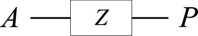
Figure 1. d-level 1-qudit gate. |
2.2. d-level M–S gates
Muthukrishnan and Stroud [6] first designed a family of 2-qudit multi-valued gates, Γ2[Zd], and its ion-trap realization. The d-level analogue of the family becomes the matrix that acts in the d2-dimensional basis of two qudits and is represented as
$\begin{eqnarray}{{\rm{\Gamma }}}_{2}[{Z}_{d}]=\left(\begin{array}{cc}{\hat{1}}_{{d}^{2}-d} & \hat{0}\\ \hat{0} & {Z}_{d}\end{array}\right).\end{eqnarray}$
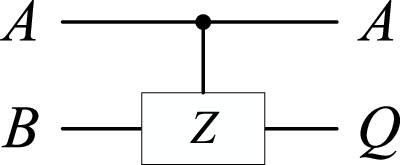
Figure 2. d-level M–S gate. |
3. Proposed multi-valued quantum gates
To design the architectures, d-level generalized Toffoli gates are derived from ternary Toffoli gates and are subsequently optimized. Additionally, d-level 2-qudit modulo addition gates are proposed to compute the sum of two input values. The specifics of these designs are elucidated in the subsequent subsections.
3.1. d-level generalized Toffoli gates
In 2007, Khan et al [29] designed the ternary Toffoli gate, a 3-qudit quantum gate. By utilizing 1-qudit and the M–S gates, it can be extended to the d-level Toffoli gate, whose first symbolic representation and realization are shown in figure 3. The output Cout is equal to the output of the permutation Z of the input C if A = B = ∣d − 1⟩. Otherwise, Cout = C. In figure 3(b), the ancilla input ∣0⟩ is transformed into ∣d − 1⟩ through permutations Zd(0(d − 2)) and Zd((d − 2)(d − 1)) controlled by inputs A and B separately. This transformed state is then utilized to control the gate Z and is restored to ∣0⟩ by the two rightmost gates. This Toffoli gate’s QC is 5; its HC is 5γ, and the NCIs is 1, where the NCIs is the number of constant-value ancilla inputs.
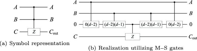
Figure 3. First implementation of d-level Toffoli gate. |
In 2020, Monfared and Haghparast [15] presented a novel implementation of the ternary Toffoli gate, which can also be extended to the d-level gate, as illustrated in figure 4. The situation shown in the figure illustrates the permutation Z as Zd(01) and the input C as the constant input ∣0⟩. This Toffoli gate’s QC is 3; its HC is 3γ, and the NCIs is 1. However, a limitation of this gate is that it does not operate correctly if A ≠ ∣d − 1⟩, B = ∣d − 1⟩, and the third input is ∣1⟩. During the design process of the architectures, this limitation can be mitigated by rearranging the order of some quantum gates so that the Toffoli gates discussed later in the paper are implemented using the method illustrated in figure 4.
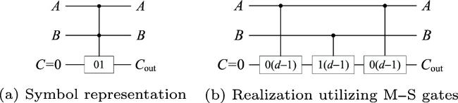
Figure 4. Second implementation of d-level Toffoli gate. |
Unlike the Toffoli gate, the states of controlling qudits in the generalized Toffoli gate are discretionary, as illustrated in figure 5. The input ∣0⟩ is transformed into ∣1⟩ by performing the permutation Zd(01) if A = ∣a0⟩ and B = ∣b0⟩, where ∣a0⟩ and ∣b0⟩ ∈ {∣0⟩, ∣1⟩, …, ∣d − 1⟩}. The generalized Toffoli gate’s QC is 7; its HC is 2ϵ + 5γ, and the NCIs is 1.
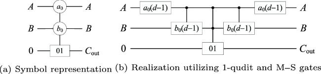
Figure 5. d-level generalized Toffoli gate. |
Both controlling qudits in the generalized Toffoli gate can be set to have multiple values. An illustrative example is provided in figure 6. The input ∣0⟩ is transformed into ∣1⟩ through the application of the permutation Zd(01) if A = ∣a0⟩ and B = ∣d − a0⟩, ∣d − a0 + 1⟩, …, or ∣d − 2⟩. The gates enclosed by the dotted line in figure 6(b) are retained if the expression (d − 2) − (d − a0) + 1( = a0 − 1) yields an odd result, whereas they are excluded if a0 − 1 is even. This generalized Toffoli gate’s QC is given by the expression 2a0 + 1 + 4h, where h equals 1 if a0 − 1 is odd and 0 if a0 − 1 is even; its HC is expressed as 2ϵ + (2a0 − 1 + 4h)γ, and the NCIs is equal to 1.
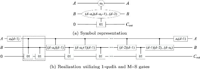
Figure 6. Another d-level generalized Toffoli gate. |
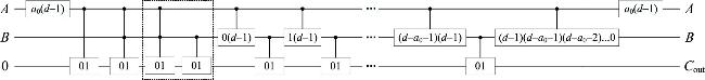
Figure 7. Different realization of the d-level generalization Toffoli gate. |
The part of figure 7 delineated by the dotted line is preserved if the expression (d − a0 − 1) + 1, which simplifies to d − a0, is odd, and it is discarded if d − a0 is even. Since there is a portion of the circuit in both figures 6 and 7 that can be either retained or discarded, the optimization of the gate can be analyzed across four distinct scenarios, as shown in table 1. For the optimization to be valid, 4a0 − 2d needs to be greater than 0, 2, 4, and 6, respectively.
Table 1. Four optimization cases. |
| Cases | a0 − 1 | d − a0 | Reduced QC | Reduced HC |
|---|---|---|---|---|
| 1 | odd | odd | 4a0 − 2d | (4a0 − 2d)γ |
| 2 | odd | even | 4a0 − 2d − 2 | (4a0 − 2d − 2)γ |
| 3 | even | odd | 4a0 − 2d − 4 | (4a0 − 2d − 4)γ |
| 4 | even | even | 4a0 − 2d − 6 | (4a0 − 2d − 6)γ |
3.2. d-level 2-qudit modulo addition gates
To calculate the modulo sum of two input values, d-level 2-qudit modulo addition gates (MAd gates) are designed, based on [26]. Let a, b ∈ {1, 2, …, d − 1}, gcd(a, d) = 1, b1 = gcd(b, d) ≥ 2, and d1 = d/b1. The MAd gate’s symbol representation and realization using 1-qudit and M–S gates are shown in figure 8, where ${a}_{d}:= a\,\mathrm{mod}\,d$. The output is defined as ${S}_{AB}:= (A+B)\,\mathrm{mod}\,d$. The gate’s QC is 2d − 2 and its HC is (d − 1)ϵ + (d − 1)γ.
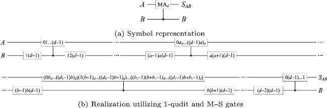
Figure 8. d-level 2-qudit modulo addition gate. |
In figure 8(b), by categorizing the values of B, the action performed on the input A can be divided into two cases as follows.
Case 1: If B = ∣a⟩, the second M–S gate drawn in the figure transforms A into (A + a)d.
Case 2: If B = ∣b⟩, the third M–S gate drawn in the figure, which corresponds to b1 permutations, transforms A into (A + b)d. In these b1 permutations, the u-th permutation transforms ∣((u − 1) + vb)d⟩ into ∣((u − 1) + (v + 1)b)d⟩, where u = 1, 2, …, d1 − 1 and v = 0, 1, …, b1 − 1.
It is noteworthy that if d = 4, gates Z4((01)(23)), Z4((02)(13)), and Z4((03)(12)) correspond to gates Z4( + 1), Z4( + 2), and Z4( + 3), respectively. The operations +1, +2, and +3 are defined within the quaternary Galois field, namely GF(4).
4. Universal architectures for multi-valued quantum adder circuits
Based on four parameters for evaluating circuit efficiency, including the QC, HC, NCIs, and NGOs, we propose the designs of universal architectures for multi-valued quantum half-adder, full-adder, parallel adder, and parallel adder/subtractor circuits in this section.
4.1. Universal architecture for multi-valued quantum half-adder circuits
A d-level quantum half-adder circuit typically accepts two d-level 1-qudit inputs, designated as A and B, and generates two outputs: the carry Cout and the sum SAB. The truth table for the d-level quantum half-adder circuit is presented in table 2. Based on [26], the realization of the universal architecture for multi-valued quantum half-adder circuits is presented in figure A1 in the appendix . For simplicity of design, all generalized Toffoli gates within this architecture are constructed in accordance with the methodology demonstrated in figure 6.
Table 2. Truth table of d-level quantum half-adder. |
| A | B | Cout | SAB |
|---|---|---|---|
| ∣0⟩ | ∣0⟩ | ∣0⟩ | ∣0⟩ |
| ∣0⟩ | ∣1⟩ | ∣0⟩ | ∣1⟩ |
| ⋮ | ⋮ | ⋮ | ⋮ |
| ∣0⟩ | ∣d − 1⟩ | ∣0⟩ | ∣d − 1⟩ |
| ∣1⟩ | ∣0⟩ | ∣0⟩ | ∣1⟩ |
| ∣1⟩ | ∣1⟩ | ∣0⟩ | ∣2⟩ |
| ⋮ | ⋮ | ⋮ | ⋮ |
| ∣1⟩ | ∣d − 1⟩ | ∣1⟩ | ∣0⟩ |
| ⋮ | ⋮ | ⋮ | ⋮ |
| ∣d − 1⟩ | ∣0⟩ | ∣0⟩ | ∣d − 1⟩ |
| ∣d − 1⟩ | ∣1⟩ | ∣1⟩ | ∣0⟩ |
| ⋮ | ⋮ | ⋮ | ⋮ |
| ∣d − 1⟩ | ∣d − 1⟩ | ∣1⟩ | ∣d − 2⟩ |
To enhance the clarity of the architecture through symbolic representation, the eleven quantum gates delineated by dotted lines in the architecture are collectively denoted as operation N, as illustrated in figure 9. Operation N is capable of computing the carry in the addition process if at least one of A and B is equal to ∣d − 1⟩, or if both are equal to ∣d − 2⟩. It is important to highlight that within this architecture, there is a controlled gate Zd(0(d − 1). . . 1) in operation N whose action encompasses the functionality of the controlled gate Zd(0(d − 1). . . 1) in the MAd gate. Consequently, to eliminate redundancy, the corresponding gate in the MAd gate should be omitted from the architecture. This modification can also be visualized as placing the final M–S gate of the MAd gate into the last dashed box. The notation for the architecture is depicted in figure 10. It is noteworthy that this architecture is not applicable to the ternary quantum half-adder circuit; thus, the architectures discussed herein pertain specifically to the case where d > 3.
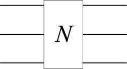
Figure 9. Operation N. |
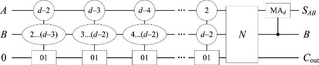
Figure 10. Universal architecture for multi-valued quantum half-adder circuits. |
When calculating the QC and HC of the architecture, the calculation results may vary if the value range and parity of level d are different. To facilitate accurate and straightforward calculations of the QC and HC, several parameters will be introduced. Specifically, let the parameter s be 0 for d = 4 and 1 for d > 4; the parameter m equal 0 if d is odd and 1 if d is even, and the parameter l take on a value of 0 for 4 ≤ d ≤ 6 and a value of 1 for d > 6. The architecture’s QC is expressed as s(d2 − 3d + 1) + 2d + 8 + 2l(d − 3 − 3m); its HC is given by (s(d − 2) + d + 1)ϵ + (s(d2 − 4d + 3) + d + 7 + 2l(d − 3 − 3m))γ; the NCIs is set to 1, and the NGOs is also 1, where the NGOs represent the number of unused outputs. In order to facilitate clarity of expression, note that
$\begin{eqnarray}\begin{array}{rcl}{t}_{0} & = & s({d}^{2}-3d+1),\\ {t}_{1} & = & 2d+8,\\ {t}_{2} & = & 2l(d-3-3m),\\ {t}_{3} & = & s(d-2)+d+1,\\ {t}_{4} & = & s({d}^{2}-4d+3).\end{array}\end{eqnarray}$
So the QC of the architecture is t0 + t1 + t2, and its HC is t3ϵ + (t1/2 + t2 + t4 + 3)γ.4.2. Universal architecture for multi-valued quantum full-adder circuits
A d-level quantum full-adder circuit is constructed upon the circuit of a half-adder, incorporating an additional input known as the low carry Cin. The corresponding truth table is provided in table 3. In figure 11, we present the symbolic representation of the universal architecture for multi-valued quantum full-adder circuits. The architecture’s QC is expressed as t0 + t1 + t2 + 6; its HC is represented as (t3 + 2)ϵ + (t1/2 + t2 + t4 + 7)γ; the NCIs is 1, and the NGOs is 2.
Table 3. Truth table of d-level quantum full-adder. |
| A | B | Cin | Cout | S |
|---|---|---|---|---|
| ∣0⟩ | ∣0⟩ | ∣0⟩ | ∣0⟩ | ∣0⟩ |
| ∣0⟩ | ∣1⟩ | ∣0⟩ | ∣0⟩ | ∣1⟩ |
| ⋮ | ⋮ | ⋮ | ⋮ | ⋮ |
| ∣0⟩ | ∣d − 1⟩ | ∣0⟩ | ∣0⟩ | ∣d − 1⟩ |
| ∣1⟩ | ∣0⟩ | ∣0⟩ | ∣0⟩ | ∣1⟩ |
| ∣1⟩ | ∣1⟩ | ∣0⟩ | ∣0⟩ | ∣2⟩ |
| ⋮ | ⋮ | ⋮ | ⋮ | ⋮ |
| ∣1⟩ | ∣d − 1⟩ | ∣0⟩ | ∣1⟩ | ∣0⟩ |
| ⋮ | ⋮ | ⋮ | ⋮ | ⋮ |
| ⋮ | ⋮ | ⋮ | ⋮ | ⋮ |
| ∣d − 1⟩ | ∣0⟩ | ∣0⟩ | ∣0⟩ | ∣d − 1⟩ |
| ∣d − 1⟩ | ∣1⟩ | ∣0⟩ | ∣1⟩ | ∣0⟩ |
| ⋮ | ⋮ | ⋮ | ⋮ | ⋮ |
| ∣d − 1⟩ | ∣d − 1⟩ | ∣0⟩ | ∣1⟩ | ∣d − 2⟩ |
| ∣0⟩ | ∣0⟩ | ∣1⟩ | ∣0⟩ | ∣1⟩ |
| ∣0⟩ | ∣1⟩ | ∣1⟩ | ∣0⟩ | ∣2⟩ |
| ⋮ | ⋮ | ⋮ | ⋮ | ⋮ |
| ∣0⟩ | ∣d − 1⟩ | ∣1⟩ | ∣1⟩ | ∣0⟩ |
| ∣1⟩ | ∣0⟩ | ∣1⟩ | ∣0⟩ | ∣2⟩ |
| ∣1⟩ | ∣1⟩ | ∣1⟩ | ∣0⟩ | ∣3⟩ |
| ⋮ | ⋮ | ⋮ | ⋮ | ⋮ |
| ∣1⟩ | ∣d − 1⟩ | ∣1⟩ | ∣1⟩ | ∣1⟩ |
| ⋮ | ⋮ | ⋮ | ⋮ | ⋮ |
| ⋮ | ⋮ | ⋮ | ⋮ | ⋮ |
| ∣d − 1⟩ | ∣0⟩ | ∣1⟩ | ∣1⟩ | ∣0⟩ |
| ∣d − 1⟩ | ∣1⟩ | ∣1⟩ | ∣1⟩ | ∣1⟩ |
| ⋮ | ⋮ | ⋮ | ⋮ | ⋮ |
| ∣d − 1⟩ | ∣d − 1⟩ | ∣1⟩ | ∣1⟩ | ∣d − 1⟩ |
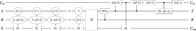
Figure 11. Universal architecture for multi-valued quantum full-adder circuits. |
4.3. Universal architecture for multi-valued quantum parallel adder circuits
A d-level, n-digit quantum parallel adder circuit is typically employed to perform the addition of two d-level n-digit numbers. The schematic representation of this circuit is illustrated in figure 12. The modules labeled FA denote a quantum full-adder circuit. The inputs are designated as C0, Ap, and Bp, where p = 0, 1, …, n − 1. The outputs are represented as Cn and Sp.
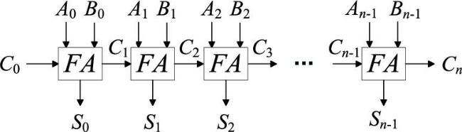
Figure 12. Schematic of the d-level, n-digit quantum parallel adder circuit. |
In figure 13, we present the symbolic representation of the universal architecture for multi-valued, 2-digit quantum parallel adder circuits. The architecture’s QC is 2t0 + 2t1 + 2t2 + 12; its HC is (2t3 + 4)ϵ + (t1 + 2t2 + 2t4 + 14)γ; the NCIs is 2, and the NGOs is 4.
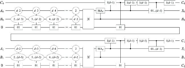
Figure 13. Universal architecture for multi-valued, 2-digit quantum parallel adder circuits. |
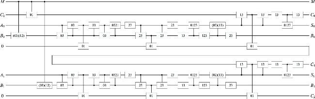
4.4. Universal architecture for multi-valued quantum parallel adder/subtractor circuits
Utilizing the methodology outlined in [7], a universal architecture for a multi-valued quantum parallel adder/subtractor circuit can be developed based on the d’s complement signed number system. The d’s complement of a number can be gated by computing the (d − 1)’s complement of the given number and subsequently adding 1 to the least significant digit. The (d − 1)’s complement of a d-level digit is shown in table 4. In a quantum circuit, this computation can be performed by applying the permutation Zd((0(d−1))(1(d−2))...(⌊(d−1)/2⌋d/2)) to a qudit.
Table 4. (d − 1)’s complement of a d-level digit. |
| Digit | 0 | 1 | … | d − 1 |
|---|---|---|---|---|
| (d − 1)’s complement | d − 1 | d − 2 | … | 0 |
Using this concept, the symbolic representation of the universal architecture for multi-valued, 2-digit quantum parallel adder/subtractor circuits can be constructed, as displayed in figure 14. The architecture operates as a parallel adder circuit if M ≠ ∣d − 1⟩ and as a parallel subtractor circuit if M = ∣d − 1⟩. Its QC is 2t0 + 2t1 + 2t2 + 15; its HC is (2t3 + 4)ϵ + (t1 + 2t2 + 2t4 + 17)γ; the NCIs is 2, and the NGOs is 5.
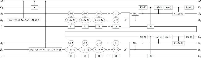
Figure 14. Universal architecture for multi-valued, 2-digit parallel adder/subtractor circuits. |
According to the data given earlier, the four parameters of the universal architectures for multi-valued quantum circuits are shown in table 5.
Table 5. Four parameters of the universal architectures. |
| Universal architectures | QC | HC | NCIs | NGOs |
|---|---|---|---|---|
| Half-adder | ${\sum }_{i=0}^{2}{t}_{i}$ | t3ϵ + (t1/2 + t2 + t4 + 3)γ | 1 | 1 |
| Full-adder | $6+{\sum }_{i=0}^{2}{t}_{i}$ | (t3 + 2)ϵ + (t1/2 + t2 + t4 + 7)γ | 1 | 2 |
| Parallel adder | $12+2{\sum }_{i=0}^{2}{t}_{i}$ | 2(t3 + 2)ϵ + 2(t1/2 + t2 + t4 + 7)γ | 2 | 4 |
| Parallel adder/subtractor | $15+2{\sum }_{i=0}^{2}{t}_{i}$ | 2(t3 + 2)ϵ + (2(t1/2 + t2 + t4 + 7) + 3)γ | 2 | 5 |
5. Comparisons and results
In light of the extensive research on ternary and quaternary adder circuits present in the current literature regarding multi-valued adder circuits, and given that the universal architectures proposed in this paper are exclusively applicable to quaternary and higher-valued circuits, the comparisons will be focused specifically on quaternary adder circuits. The realizations of the quaternary adder circuits derived from these architectures are shown in figures A2 to A5 in the appendix .
The less QC and HC, and the fewer NCIs, and NGOs a circuit has, the more effective it is [25]. Comparisons of different adder circuits in terms of QC, HC, NCIs, and NGOs are illustrated in tables 6 to 9. As indicated by the data in the tables, the proposed circuits outperform the circuits in the referenced papers in all four parameters. From tables 6 to 9, it can be concluded that the QC of the proposed quaternary half-adder, full-adder, parallel adder, and parallel adder/subtractor is approximately 5.8%, 4.3%, 70.2%, and 68.9% lower than that of the current quaternary adders with the lowest QC, respectively. Additionally, the NCIs and NGOs of the former are not greater than those of the latter. Furthermore, upon analyzing tables 5 to 9, it is noteworthy that the NCIs and NGOs of the proposed universal architectures are the same as those of the quaternary adders generated from them, and do not vary with the change of the level d. This implies that any multi-valued quantum adder can be constructed with the lowest NCIs and NGOs using the proposed universal architectures.
Table 6. Comparison of half-adders. |
Table 7. Comparison of full-adders. |
Table 8. Comparison of parallel adders. |
6. Conclusion
When the qudit levels can be discretionary, a trade-off exists between the quantity of qudits that constitute a quantum computer and the number of levels associated with each qudit. This trade-off changes depending on the specific problems being addressed. Consequently, it is essential to design fundamental components, such as quantum adders, in a manner that allows for their application across different qudit levels.
We propose a universal architecture for multi-valued quantum half-adder circuits using four types of quantum gates: the d-level 1-qudit gate, the M–S gate, the generalized Toffoli gate, and the 2-qudit MAd gate. Additionally, universal architectures for multi-valued full-adder, parallel adder, and parallel adder/subtractor circuits are derived based on this proposal. These architectures are all applicable to quaternary and higher-valued circuits.
To illustrate the efficacy of these architectures, quaternary adder circuits derived from them are proposed and compared with several current counterparts. These circuits exhibit lower QC, HC, NCIs, and NGOs than those reported in previous studies. Additionally, multi-valued adder circuits derived from these architectures can be adapted for use in quantum systems of corresponding levels, thereby serving as fundamental components in various algorithms.
Appendix. Realizations of the adder circuits
In figures A1 to A5, we present the realizations of the universal architecture for multi-valued quantum half-adder circuits and four quaternary quantum adders derived from the architectures, respectively.
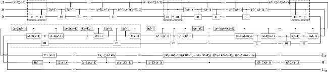
Figure A1. Universal architecture for multi-valued quantum half-adder circuits. |
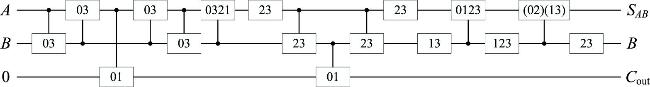
Figure A2. Quaternary quantum half-adder circuit. |
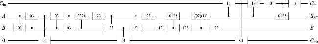
Figure A3. Quaternary quantum full-adder circuit. |
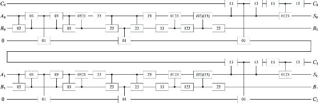
Figure A4. Quaternary quantum parallel adder circuit. |
Figure A5. Quaternary quantum parallel adder/subtractor circuit. |