


1. Introduction
At the end of the 20th century, two research teams reported the transformative giant magnetoresistance (GMR) effect in Fe/Cr(001) multilayers and in Fe/Cr/Fe(001) trilayers [1, 2]. It unveiled that electron transport in ferromagnetic materials is highly dependent on spin states. This phenomenon stems from spin-polarized band splitting. This quantum mechanical effect serves as the fundamental basis for the substantial resistance variations that are observed as alternating magnetic layers transition between parallel and antiparallel magnetization configurations. The technological influence of GMR has been profoundly transformative, bringing about significant changes in relevant fields [3-20]. Beyond revolutionizing data storage with ultra-sensitive read heads, GMR-based devices have become ubiquitous across multiple sectors. In automotive systems, they are utilized in wheel speed sensors; in biomedical diagnostics, they enable the detection of magnetic nanoparticles, and in space exploration, they are deployed as radiation-hardened current monitors. Moreover, the GMR effect laid the groundwork for spintronics, an emerging field that harnesses spin-dependent transport, expanding beyond the traditional realm of charge-based electronics. Recent advancements in graphene nanoribbons (GNRs) vividly illustrate this trend. The edge-dependent electronic states and tunable bandgaps of GNRs enable spin-filtered quantum tunneling under electrostatic or magnetic gating. This behavior resembles that of semiconductor-based giant magnetoresistance (GMR) devices, yet GNRs exhibit superior spin coherence. Significantly, in the context of this study, GNRs modulated by δ-doping display resonant transmission peaks closely associated with magnetic anisotropy. These findings provide novel design guidelines for developing spintronic devices with ultrahigh magnetoresistance ratios (MRR) [21].
The exploration of hybrid ferromagnetic/semiconductor GMR devices commenced with the work of Zhai et al [22]. They first demonstrated this effect in a GaAs/AlxGa1-xAs 2DEG heterostructure patterned with parallel ferromagnetic (FM) stripes [23]. Distinct from conventional metallic GMR systems, this architecture achieved an extraordinary magnetoresistance ratio (MRR) exceeding 106% at practical electron densities without the need for explicit spin polarization. This breakthrough originated from geometric magnetoresistance mechanisms. Subsequently, Papp et al [24, 25] further enhanced the MRR limit to approximately 1031% through the optimization of FM/semiconductor interfaces, positioning these devices as promising candidates for ultrahigh-density magnetic storage. The GMR effect in these kinds of devices is non-tunable, and thus hampering them against using in practice. Recent advances in δ-doping engineering have opened pathways for the behavior of the spin-polarized electron in the GMR device control [26-29]. For example, Zhang et al [28] and Liu et al [29] predicted in their theoretical models that adjusting the concentration or spatial location of δ-doping in GMR devices can affect the size and polarity of MRR, thereby achieving structural control of the device's magnetic response [30, 31]. In their theoretical demonstration, Zhang and Liu et al had adopted the same device structures without δ-doping as those used by Papp et al in [24, 25], however, the peak MRR and the MRR-EF curve with V = 0 case was completely different from those given in [24, 25]. To comprehensively understand the δ-doping modulation on the GMR effect and to clarify the above discrepancy, the GMR effect was reinvestigated in exactly the same model devices with δ-doping as those adopted in [28, 29] with an optimized transfer matrix. We numerically recalculated the transmission probability, the conductance and the magnetoresistance ratio with various δ-doping weights and/or positions, and successfully derived the dependence of the peak magnetoresistance ratio value and its Fermi energy position on the δ-doping weight and position with high precision computation. The results obtained without δ-doping were found to fully reproduce those results given by Papp et al in [24, 25]. Surprisingly, the results obtained with δ-doping differed greatly from those reported by Zhang et al and Liu et al in [28, 29]. We thus make clear that the whole of the results illustrated in [28, 29] are inaccurate; their inaccuracies most likely attributable to the use of the inaccurate magnetic vector potentials, and some errors of calculation. In our previous study published in [32], we explored the effect of δ-doping on GMR in a center-misaligned two-strip structure. This study further focuses on the overlapping stripe structure and systematically investigates the symmetric control effect of δ-doping position and intensity on the GMR peak and Fermi energy position.
2. Model and theoretical method
The schematic diagram of GMR device is depicted in figure 1(a). This device can be experimentally fabricated by depositing two nanosized ferromagnetic (FM) stripes on the top and bottom of a GaAs/AlxGa1-xAs 2DEG heterostructure [23, 24].
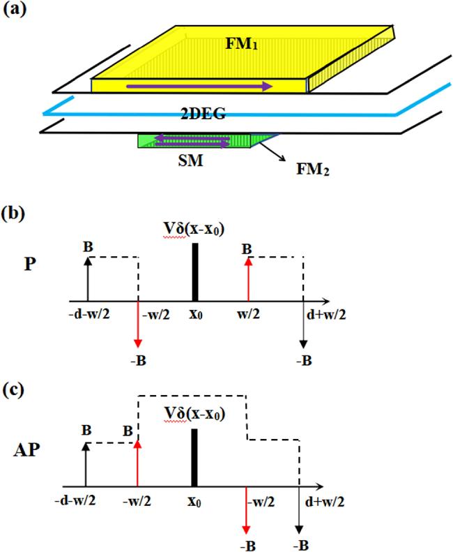
Figure 1. (a) Schematic diagram of the model GMR device: two FM stripes are deposited on top and bottom of the GaAs/AlxGa1-xAs 2DEG heterostructure, (b) P and (c) AP alignments of the device, respectively, where a δ-doping Vδ(x-x0) is comprised. |
We consider two ferromagnetic (FM) stripes aligned centrally and magnetized in-plane. Figures 1(b) and (c) illustrate the magnetic configuration in their parallel (P) and antiparallel (AP) states, respectively. Into this setup, a δ-doping potential Vδ(x-x0) is embedded, characterized by its amplitude V and offset position x0.
When the contact distance between the FM grid and the 2DEG is extremely small, the resulting magnetic shadow field can be approximated by a delta function model.
$\begin{eqnarray}\begin{array}{lll}{B}_{z}\left(x\right) & = & B\left[\delta \left(x+d+\displaystyle \frac{w}{2}\right)-\delta \left(x-d+\displaystyle \frac{w}{2}\right)\right]\\ & & -\,\chi B\left[\delta \left(x+\displaystyle \frac{w}{2}\right)-\delta \left(x-\displaystyle \frac{w}{2}\right)\right],\end{array}\end{eqnarray}$
the first bracket denotes the magnetic field generated by the top FM stripe, while the second corresponds to that from the bottom stripe. Here, B is the strength of the magnetic field, w and (w + 2d) are the width of bottom and top FM stripes respectively, with χ = ±1 represents the P and AP magnetization configurations.The effective single-particle Hamiltonian for a modulated 2DEG system in the (x, y) plane is expressed by
$\begin{eqnarray}H=\displaystyle \frac{1}{2{m}^{\ast }}{\left[\vec{p}+e\vec{A}\left(x\right)\right]}^{2}+\displaystyle \frac{e{g}^{\ast }}{2{m}_{0}}\displaystyle \frac{\sigma \hslash }{2}{B}_{z}\left(x\right)+V\delta \left(x-{x}_{0}\right),\end{eqnarray}$
where m* is the effective mass of the electron, and g* and (px, py) are the effective Landé factor and the momentum, m0 is the free electron mass, σz = +1/-1 represent spin-up/spin-down electrons.The magnetic vector potential can be given in the Landau gauge by $\vec{A}=\left(0,{A}_{y},0\right)$, and Ay is written as
$\begin{eqnarray}{A}_{y}=\left\{\begin{array}{ll}0 & x\lt -d-w/2\\ B{l}_{B} & -d-w/2\lt x\lt -w/2\\ \left(1-\chi \right)B{l}_{B} & -w/2\lt x\lt w/2\\ B{l}_{B} & w/2\lt x\lt d+w/2\\ 0 & d+w/2\lt x\end{array}\right..\end{eqnarray}$
So, the magnetic vector potentials of the two FMs are of center collinearity and overlapped, resulting in the magnetic vector potential in the region of $-w/2\lt x\lt w/2$ be eliminated to 0 with $\chi =+1$ (in P) or enhanced to 2B${l}_{B}\,$ with $\chi =-1$ (in AP). For simplicity, the dimensionless units are also introduced here with the electron cyclonic frequency ${\omega }_{c}=e{B}_{0}/{m}^{\ast }$, and the magnetic length $\,{l}_{B}=\sqrt{\hslash /e{B}_{0}}$ for an estimated magnetic field B0. And, all the relevant quantities are expressed in dimensionless units: (1) the energy $E\to \hslash {\omega }_{c}E$, (2) the δ-doping strength $V\to \left(\hslash {\omega }_{c}/e\right)V$, (3) the coordinate $\vec{r}\to {l}_{B}\vec{r}$, (4) the vector potential $\vec{A}\left(x\right)\to {B}_{0}{l}_{B}\vec{A}\left(x\right)$ and (5) the magnetic field $\vec{B}\left(x\right)\to {B}_{0}\vec{B}\left(x\right)$. For GaAs ${g}^{\ast }=0.44$ and ${m}^{* }=0.067{m}_{0}$, and for an estimated ${B}_{0}=0.1$ T, we have ${l}_{B}=81.3$ nm, $\hslash {\omega }_{c}=0.17$ meV.
Since the Hamiltonian is commutated with the momentum operator in the y-direction, the wave function of the electron can be written as $\psi \left(x,y\right)=\psi \left(x\right){{\rm{e}}}^{{\rm{i}}{k}_{y}y}$, where ${k}_{y}$ is the wave vector of the electron along the y-direction, and thus the one-dimensional Schrödinger equation can be obtained
$\begin{eqnarray}\left\{\displaystyle \frac{{{\rm{d}}}^{2}}{{\rm{d}}{x}^{2}}+2\left[E-{U}_{\mathrm{eff}}\left(x,{k}_{y},\chi ,V,\sigma ,{x}_{0}\right)\right]\right\}\psi \left(x\right)=0,\end{eqnarray}$
with $\begin{eqnarray}\begin{array}{lll}{U}_{\mathrm{eff}}\left(x,{k}_{y},\chi ,V,\sigma ,{x}_{0}\right) & = & \frac{{\left[{k}_{y}+{A}_{y}\left(x\right)\right]}^{2}}{2}\\ & & +\frac{e{m}^{\ast }{g}^{\ast }}{2{m}_{0}}\frac{\sigma \hslash }{2}{B}_{z}\left(x\right)+V\delta \left(x-{x}_{0}\right),\end{array}\end{eqnarray}$
where Ueff is the effective potential of the system, and the first item is the magnetic effective potential related to the wave vector ky, the second item is the Zeeman coupling between the electron-spin σz and the magnetic field Bz(x), $\displaystyle \frac{{m}^{\ast }{g}^{\ast }B}{4{m}_{0}}\approx 0.036$ for GaAs materials with B = 5, which is much smaller than other items in Ueff, the last item is the δ-doping potential barrier. The effective potential Ueff is modulated by the δ-doping potential barrier, and each term plays a decisive role in the nature of electron transport.Using an optimized transfer matrix method [4, 33], we obtained the relation between the reflection amplitude r and transmission amplitude t by solving equation (4 ).
$\begin{eqnarray}\left(\begin{array}{c}1\\ r\end{array}\right)=\displaystyle \frac{1}{2}\left(\begin{array}{cc}1 & -{\rm{i}}{k}_{0}^{-1}\\ 1 & {\rm{i}}{k}_{0}^{-1}\end{array}\right)M\left(\begin{array}{cc}1 & {\rm{i}}{k}_{0}\\ 1 & -{\rm{i}}{k}_{0}\end{array}\right)\left(\begin{array}{c}t\\ 0\end{array}\right),\end{eqnarray}$
where M is the global transfer matrix with 2 × 2 dimensions, which is expressed as $\begin{eqnarray}M={M}_{d}{M}_{\chi lw}{M}_{\delta }{M}_{\chi rw}{M}_{d},\end{eqnarray}$
with $\begin{eqnarray}{M}_{d}=\left(\begin{array}{cc}\cos \left({k}_{d}d\right) & -\sin \left({k}_{d}d\right)/{k}_{d}\\ {k}_{d}\,\sin \left({k}_{d}d\right) & \cos \left({k}_{d}d\right)\end{array}\right),\end{eqnarray}$
$\begin{eqnarray}{M}_{\chi lw}=\left(\begin{array}{cc}\cos \left[{k}_{\chi w}\left({x}_{0}+w/2\right)\right] & -\sin \left[{k}_{\chi w}\left({x}_{0}+w/2\right)\right]/{k}_{\chi w}\\ {k}_{\chi w}\,\sin \left[{k}_{\chi w}\left({x}_{0}+w/2\right)\right] & \cos \left[{k}_{\chi w}\left({x}_{0}+w/2\right)\right]\end{array}\right),\end{eqnarray}$
$\begin{eqnarray}{M}_{\delta }=\left(\begin{array}{cc}1 & 0\\ -2V & 1\end{array}\right),\end{eqnarray}$
$\begin{eqnarray}{M}_{\chi rw}=\left(\begin{array}{cc}\cos \left[{k}_{\chi w}\left(w/2-{x}_{0}\right)\right] & -\sin \left[{k}_{\chi w}\left(w/2-{x}_{0}\right)\right]/{k}_{\chi w}\\ {k}_{\chi w}\,\sin \left[{k}_{\chi w}\left(w/2-{x}_{0}\right)\right] & \cos \left[{k}_{\chi w}\left(w/2-{x}_{0}\right)\right]\end{array}\right),\end{eqnarray}$
$\begin{eqnarray}\begin{array}{c}{k}_{0}=\sqrt{2E-{k}_{y}^{2}},\\ {k}_{d}=\sqrt{2E-{\left(B+{k}_{y}\right)}^{2}},\\ {k}_{\chi w}=\sqrt{2E-{\left[\left(1-\chi \right)B+{k}_{y}\right]}^{2}},\end{array}\end{eqnarray}$
Thus, the transmission probability ${T}_{{\rm{\chi }}}\left(E,\,{k}_{y}\right)$ could be expressed as:
$\begin{eqnarray}{T}_{{\rm{\chi }}}\left(E,\,{k}_{y}\right)=\left\{\displaystyle \frac{4}{{\left[\left|{M}_{11}+{M}_{22}\right|\right]}^{2}+{\left[\left|{k}_{0}{M}_{12}-{M}_{21}/{k}_{0}\right|\right]}^{2}}\right\}.\end{eqnarray}$
Then, we obtain the conductance ${G}_{{\rm{\chi }}}$ using the well-known Landauer-Buttiker formula [33]:
$\begin{eqnarray}{G}_{{\rm{\chi }}}={G}_{0}\displaystyle {\int }_{-\pi /2}^{\pi /2}{T}_{{\rm{\chi }}}\left({E}_{{\rm{F}}},\sqrt{2{E}_{{\rm{F}}}}\,\sin \left(\theta \right)\right)\cos \left(\theta \right){\rm{d}}\theta ,\end{eqnarray}$
where ${E}_{{\rm{F}}}$ is the Fermi energy, $\theta $ is the angle between the incident wave vector of the electron and the x-direction, G0 represent conductance coefficient, that is $\begin{eqnarray}{G}_{0}={e}^{2}{m}^{\ast }{\upsilon }_{F}{l}_{y}/{\hslash }^{2},\end{eqnarray}$
where ${\upsilon }_{F}$ is the Fermi velocity, ${l}_{y}$ is the length of the barrier structure in the y-direction.The magnetoresistance ratio is defined as: [24, 25]
$\begin{eqnarray}{\rm{MRR}}=\displaystyle \frac{{G}_{{\rm{P}}}-{G}_{\mathrm{AP}}}{{G}_{\mathrm{AP}}}\times 100 \% ,\end{eqnarray}$
with ${G}_{{\rm{P}}}$ and ${G}_{\mathrm{AP}}$ being the conductance ${G}_{{\rm{\chi }}}$ $with\,{\rm{\chi }}=+1$ (in P) and with ${\rm{\chi }}=-1$ (in AP) alignments, respectively.3. Results and discussion
Figure 2 shows the logarithmic plot of transmission probability spectra for P and AP alignments with the δ-doping (with V = 2 and x0 = 0) and when ky = -2, 0 and 2, respectively. The huge anisotropy with the wavevector in the transmission probability spectra is due to the essentially two-dimensional (2D) process for the electron through such magnetic nanostructure. Additionally, the resonant transmission peaks with unity values are observed clearly in the case of P alignment due to the effective potential Ueff behaving as a multiple-barrier quantum-well structure. While the Ueff in the case of AP alignment behaves as multiple barriers, and the electronic transmission is strongly blocked and the resonant tunneling is excluded in the low energy region, the electron transmission through the AP arrangement has an extremely low probability compared to those of in the P arrangement. Figure 2 has perfectly repeated those reported in [28], except for that the transmission probability spectra with ky = 0 and 2 in the low energy region 0 < E < 10E0, those were omitted from figure 2(b) of [28].
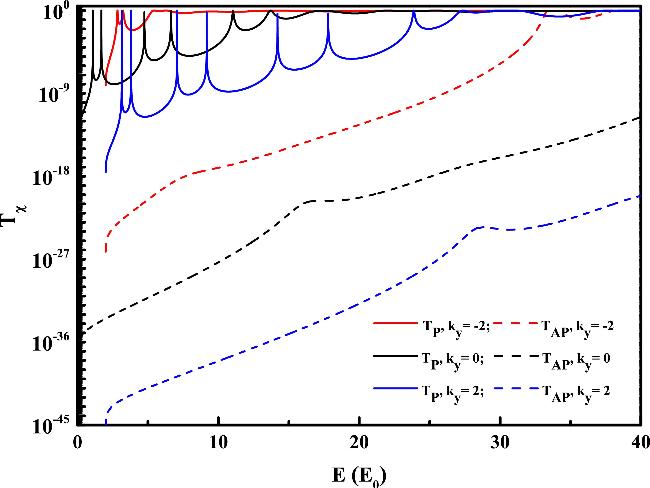
Figure 2. The logarithmic plots of the ${T}_{\chi }$ for the electron tunneling through P and AP magnetizations versus the incident energy E for ky = -2, 0, and 2, here V = 2 and x0 = 0. |
Figure 3(a) plots the conductance at both P and AP alignments versus the Fermi energy for the δ-doping (with V = 2 and x0 = 0). The GP shows several peaks due to resonant tunneling and it increases rapidly with EF going to higher energies, the striking conductance peak with a large peak-to-valley ratio appeared at Fermi energy EF ~ 6.5E0. For the AP alignment, the transmission is blocked drastically and the corresponding conductance GAP is almost zero. There is a large difference in conductance between the P and AP alignments in a wide region of low Fermi energies, where GAP is close to zero whereas GP is finite. This great discrepancy between GP and GAP generates the apparent GMR effect. Figure 3(b) shows the corresponding curve of MRR versus Fermi energy EF. The MRR with δ-doping of (V = 2, x0 = 0) displays an extremely sharp peak of 3.2 × 1029% at the Fermi energy of 1.08E0, and the peak MRR is greatly reduced compared to the case without δ-doping. This high MRR stems from its definition: GAP, the denominator term, is much smaller relative to GP, which is much smaller than GP. While the extremely high MRR values, reaching 1030%, are theoretically consistent with the sharp suppression of GAP, we acknowledge that such values might appear unrealistic under experimental conditions. These results stem from the idealized model employed in this work, which assumes perfect material conditions, negligible thermal effects, and high computational precision. In practical scenarios, factors such as material imperfections, finite temperature, and noise could moderate these extreme values. Nevertheless, these findings provide valuable theoretical insights into the tunability of GMR devices and highlight the potential impact of δ-doping modulation. Although figure 3(a) has almost repeated those reported in [28, 29], the MRR versus Fermi energy EF, as shown in figure 3(b), are completely different from those given in [28, 29]. The differences are highly significant in not only the MRR value, but also in the shape of MRR-EF curve. The conductance and the MRR of the GMR device of the same structural parameters without doping have been reported in [22, 23] by Papp and Borza, the shapes of both our conductance and MRR-EF curve look similar to those described in [24, 25]. Thus, we believe that those results illustrated as inserted in figure 2(b) of [28] and as inserted in figure 3(b) of [29] are inaccurate, which may result from some overlooked errors in their numerical calculation process.
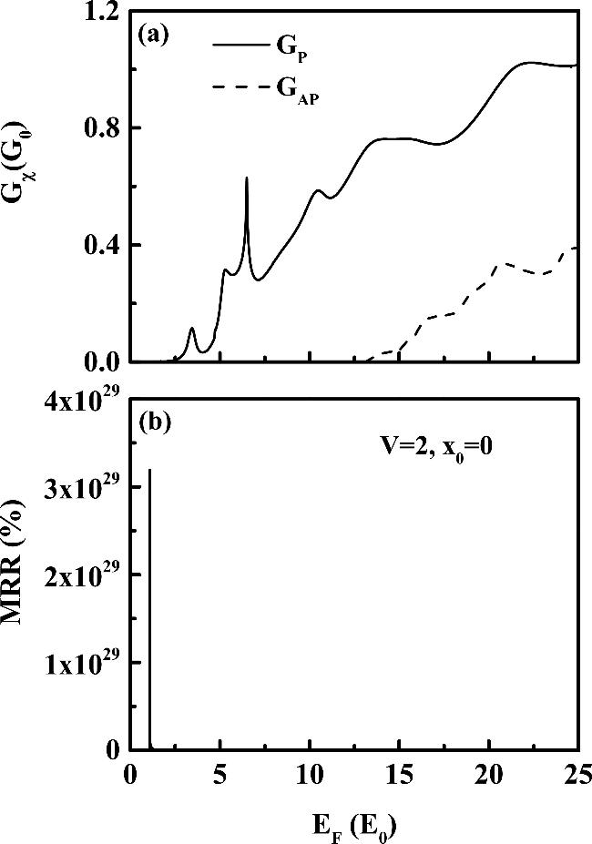
Figure 3. (a) Plots GP (solid) and GAP (dashed) for P and AP alignments versus the Fermi energy EF; (b) gives the corresponding MRR versus Fermi energy EF, here V = 2 and x0 = 0. |
Figures 4(a)-(c) plot the curves of the MRR versus the Fermi energy EF with the weight of the δ-doping V = 0, 2 and 4 with the δ-doping being fixed at position x0 = 0. For all three MRR-EF curves with different strengths of δ-doping, each curve displays an extremely sharp peak. The MRR-EF curve shifts obviously to higher energy while the peak MRR apparently decreases as the V becomes larger. For the δ-doping strength V = 0 to 2 and 4, the peak MRR appears at Fermi energy of 0.426E0 to 1.083E0, and1.308E0, and the MRR peak values reach up to 1.83 × 1032% to 3.19 × 1029% and 6.72 × 1028%, respectively. Figure 4(d) gives the MRR as a function of the V with the Fermi energy being fixed at EF = 6 and with the δ-doping being fixed at position x0 = 0. The MRR(EF = 6)-V curve increases monotonously with V increasing from -5 to 5, and the MRR value increases faster in the region from -5 to 0 than that in the region from 0 to 5. Once again, it is obvious that our results obtained here are very much different from those illustrated in [28, 29]. However, our MRR-EF curve with V = 0 is almost a copy of that reported in [24] by Papp et al without the δ-doping. The relative lower peak MRR value of ~1031% is a direct result of their low numerical precision and the wide energy step adopted in their numerical calculations. These interesting findings further confirm that those MRR-EF and the MRR(EF = 6)-V given in [28, 29] are inaccurate. The tunability of the GMR device observed in this study bears resemblance to similar modulation phenomena in graphene nanoribbons, where electrostatic gating or magnetic barriers are employed to control tunneling and transmission properties. While graphene nanoribbons offer higher carrier mobility and unique edge-state effects, δ-doping in semiconductor systems provides precise and stable control of the effective potential landscape. This makes δ-doping a promising alternative for applications such as magnetic sensing and information storage, where structural tunability is critical. Comparing the results of this study with recent findings in graphene nanoribbon systems highlights the complementary strengths of these approaches in quantum transport research.
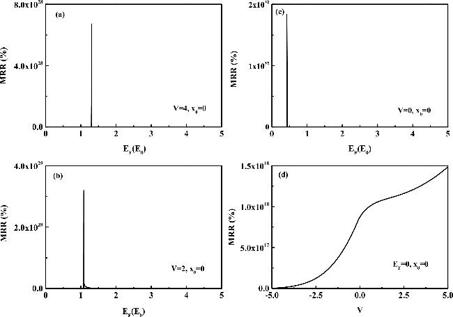
Figure 4. (a)-(c) Plots the curves of the MRR versus the Fermi energy EF with the weight of the δ-doping V = 0, 2 and 4 with x0 = 0. (d) gives the MRR versus the weight of the δ-doping V at EF = 6.0. |
As shown in figure 5, at a fixed δ-doping position, x0 = 0. decreasing the δ-doping intensity V causes the peak MRR to increase exponentially (from approximately 1028% to 1035%), while the Fermi energy shifts significantly downward (from 1.37E0 to 0.075E0). When V decreases below -0.5, the MRR peak disappears and the Fermi energy enters the negative region. This phenomenon arises from the suppression of P-configuration transmission under positive δ-doping, while AP-configuration transmission is nearly forbidden under negative δ-doping. Clearly, the dependence of MRR on V can be explained by Ueff(V), indicating that the δ-doping intensity is a key parameter in modulating GMR device performance.
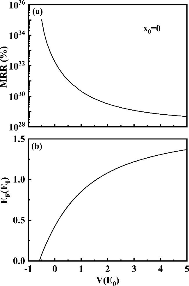
Figure 5. (a) Plots the peak MRR and (b) its Fermi energy position versus the δ-doping strength V, here x0 = 0. |
Figures 6(a)-(c) plot the MRR as a function of Fermi energy EF with five different δ-doping positions x0 = 0, ±1 and ±2, respectively, here the weight of the δ-doping is fixed at V = 2. The MRR-EF curve strongly depends on the δ-doping position. The MRR curves with ±x0 overlap each other, which is a direct reflection of the intrinsic inversion-symmetry of the effective potential Ueff, which shows spatial inversion-symmetry for the P or the AP alignments. For the δ-doping position of x0 = 0 to ±1 and ±2, the MRR peak appears at Fermi energies of 0.426E0 to 0.589E0, and 1.083E0, with the peak values of 1.83 × 1029% to 9.85 × 1030% and 3.10 × 1032%, respectively. With the δ-doping being shifted from the center to the magnetic barriers, the peak MRR value increases exponentially with Fermi energy position being shifted greatly to lower energy. Figure 6(d) gives the MRR as a function of the position of the δ-doping x0 with the Fermi energy fixed at EF = 6.0. The MRR dependence on the δ-doping position shows inversion-symmetry with respect to the x0, i.e., MRR(x0) = MRR(-x0). Again, the MRR-EF curves with five different δ-doping positions x0 and the MRR(EF = 6)-x0 given in [28, 29] are found to be inaccurate, the differences are clearly observable in the MRR-EF curve shapes, the peak MRR value and its Fermi energy positions.
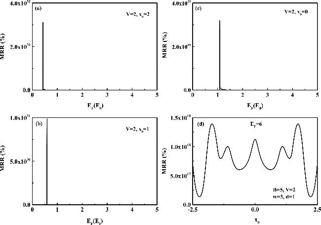
Figure 6. (a)-(c) Plot the MRR versus the Fermi energy EF with five different δ-doping positions x0 = 0, ±1 and ±2, respectively, here the weight of the δ-doping is fixed at V = 2. (d) Plots the MRR versus the position of the δ-doping x0 at EF = 6. |
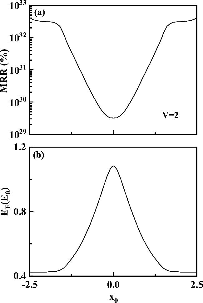
Figures 7(a) and (b) plot the dependence of the peak MRR value and its Fermi energy position on the δ-doping position x0, with the weight of the δ-doping being fixed at V = 2. Indeed, the peak MRR value and its Fermi energy position vary drastically with the δ-doping x0 and shows a symmetric behavior pertaining to the x0. Both the peak MRR increases and its Fermi energy position decrease rapidly when the δ-doping is gradually shifted from the center to the inner edges of magnetic barriers, i.e., $0\leqslant \left|{x}_{0}\right|\leqslant w/2$. When the δ-doping enters the magnetic barrier regions and is shifted from the inner to the outer edges of the magnetic barriers, i.e., $w/2\leqslant \left|{x}_{0}\right|\,\leqslant \left(w/2+{\rm{d}}\right)$, the magnitudes of both the peak MRR increase or its Fermi energy position decrease become extremely small. The MRR peak reaches the minimum when the δ-doping is situated at the center of the device, i.e., x0 = 0, while the MRR peak reaches the maximum when the δ-doping is placed at the outer edges of the magnetic barriers, i.e., x0 = ±(w/2 + d). These results indicate that one can also modulate the performance of the GMR device by properly adjusting the δ-doping position.
Figure 7. (a) and (b) plot peak MRR value and its Fermi energy position versus the δ-doping position x0, here V = 2. |
4. Conclusions
By employing an optimized transfer matrix method, we performed a systematic numerical study of δ-doping effects on transmission probability, conductance, and MRR in a 2DEG heterostructure with two overlapping magnetic barriers. Our high-precision computational analysis provides quantitative insights into the interplay among peak MRR, Fermi energy position, and δ-doping parameters (strength and position). Notably, our findings demonstrate that the peak MRR value and its corresponding Fermi energy position exhibit symmetry with respect to the position x0. As the δ-doping strength increases, the peak MRR value decreases exponentially, with its Fermi energy position shifting significantly toward higher energies. Conversely, as the δ-doping position shifts from the center of the magnetic barriers toward their outer edges, the peak MRR value increases exponentially, accompanied by a pronounced shift of the Fermi energy position toward lower energies. The results demonstrate that precise optimization of the δ-doping configuration significantly enhances GMR device performance. Our findings align closely with theoretical predictions and reveal inaccuracies in prior computational studies. Our study provides valuable quantitative guidance for controlling the MRR of GMR devices through δ-doping, which is expected to be highly beneficial for the design of structurally tunable GMR devices.